Process for producing a nanoelement arrangement, and nanoelement arrangement

a nanoelement and nanoelement technology, applied in the direction of pulse technique, instruments, computation using denominational number representation, etc., can solve the problems of limited scaleability of storage media, inability to control the spatially defined formation of branched carbon nanotubes, and the limit of conventional silicon microelectronics, etc., to achieve good spatial definition, improve electrical contact resistance, and improve the effect of branching point electrical properties

Inactive Publication Date: 2005-02-24
POLARIS INNOVATIONS
View PDF2 Cites 37 Cited by
  • Summary
  • Abstract
  • Description
  • Claims
  • Application Information

AI Technical Summary

Benefits of technology

[0030] The catalyst material between the first and the at least one second nanoelement can then be nickel-plated, i.e., provided with nickel material at least at the surface. To improve an electrical contact resistance at the branching location between a first and a second nanoelement, it is possible, for example when iron material is used as catalyst material, to carry out a wet-chemical, electroless nickel-plating at the branching point, which is catalyzed by the existing iron material, in order to improve the electrical properties of the branching point.
[0031] A partial region of the first nanoelement can be covered with a protective layer, which preferably has no catalytic action for the growth of nanoelements. In other words, the material of the protective layer is preferably selected in such a way that nanoelements cannot grow or can only grow to a slight extent on the protective layer. In such a case, significant growth of...

Problems solved by technology

With ongoing miniaturization, conventional silicon microelectronics will reach its limit.
In addition to the problems which arise in an individual component, a further difficulty in a memory arrangement is a limited scaleability of the storage medium, for example the capacitance in a DRAM (dynam...

Method used


Image

  • Process for producing a nanoelement arrangement, and nanoelement arrangement
  • Process for producing a nanoelement arrangement, and nanoelement arrangement
  • Process for producing a nanoelement arrangement, and nanoelement arrangement

Examples


Embodiment Construction

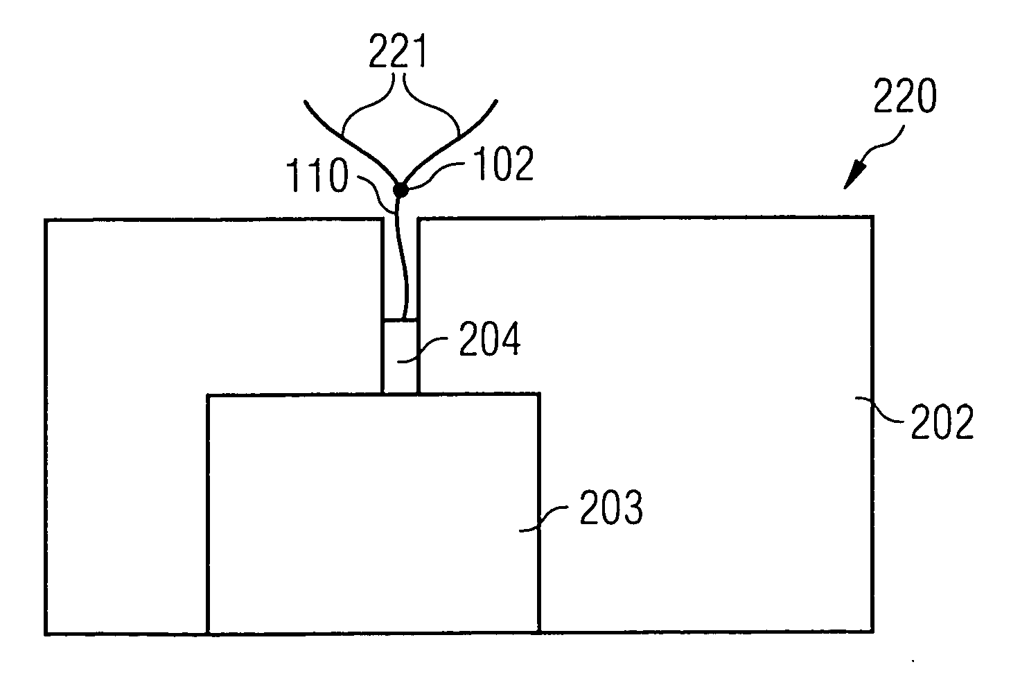
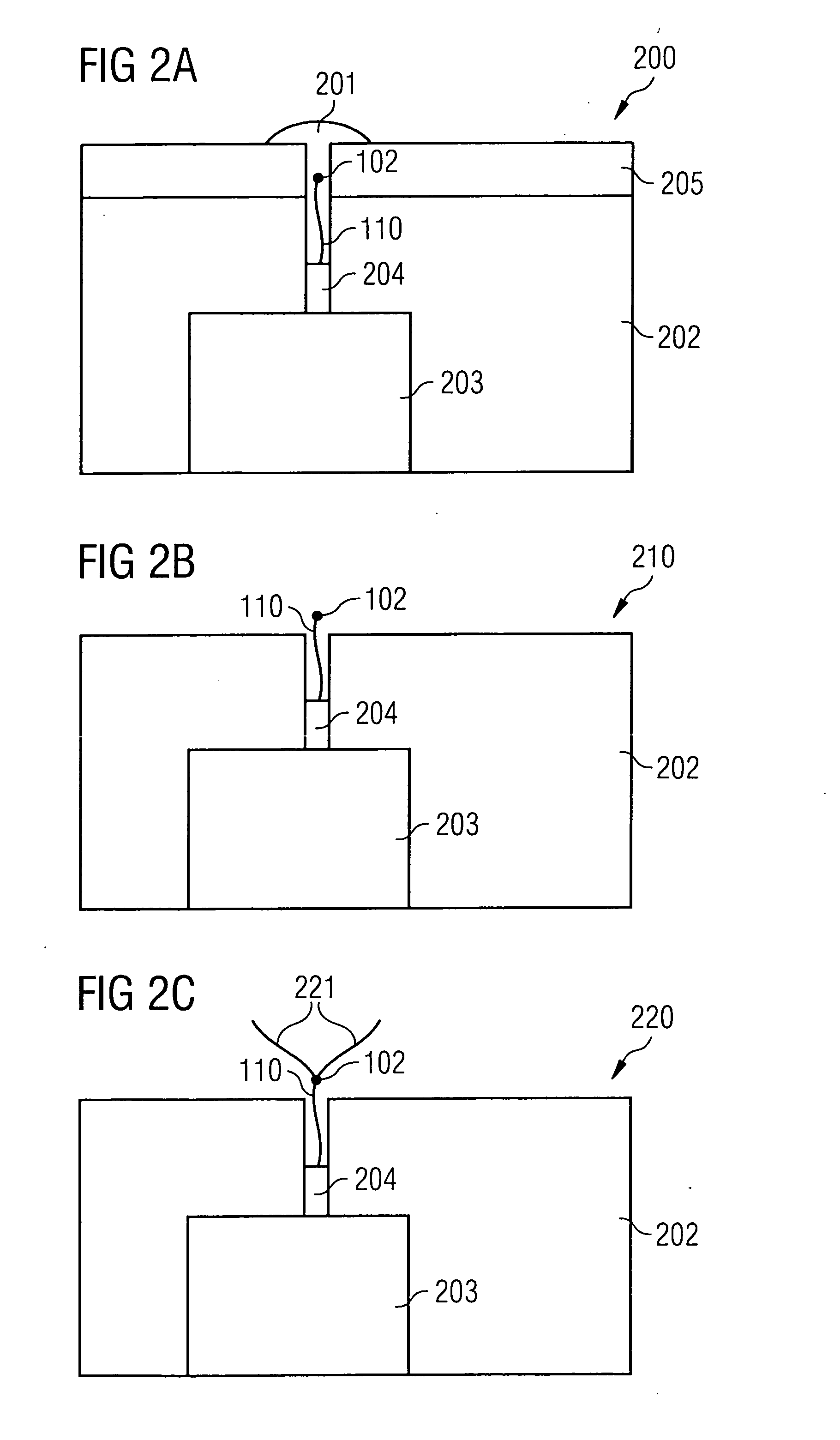
[0056] The text which follows describes, with reference to FIG. 1A, FIG. 1B, FIG. 2A to FIG. 2C, a process for producing a carbon nanotube arrangement in accordance with a preferred exemplary embodiment of the invention.

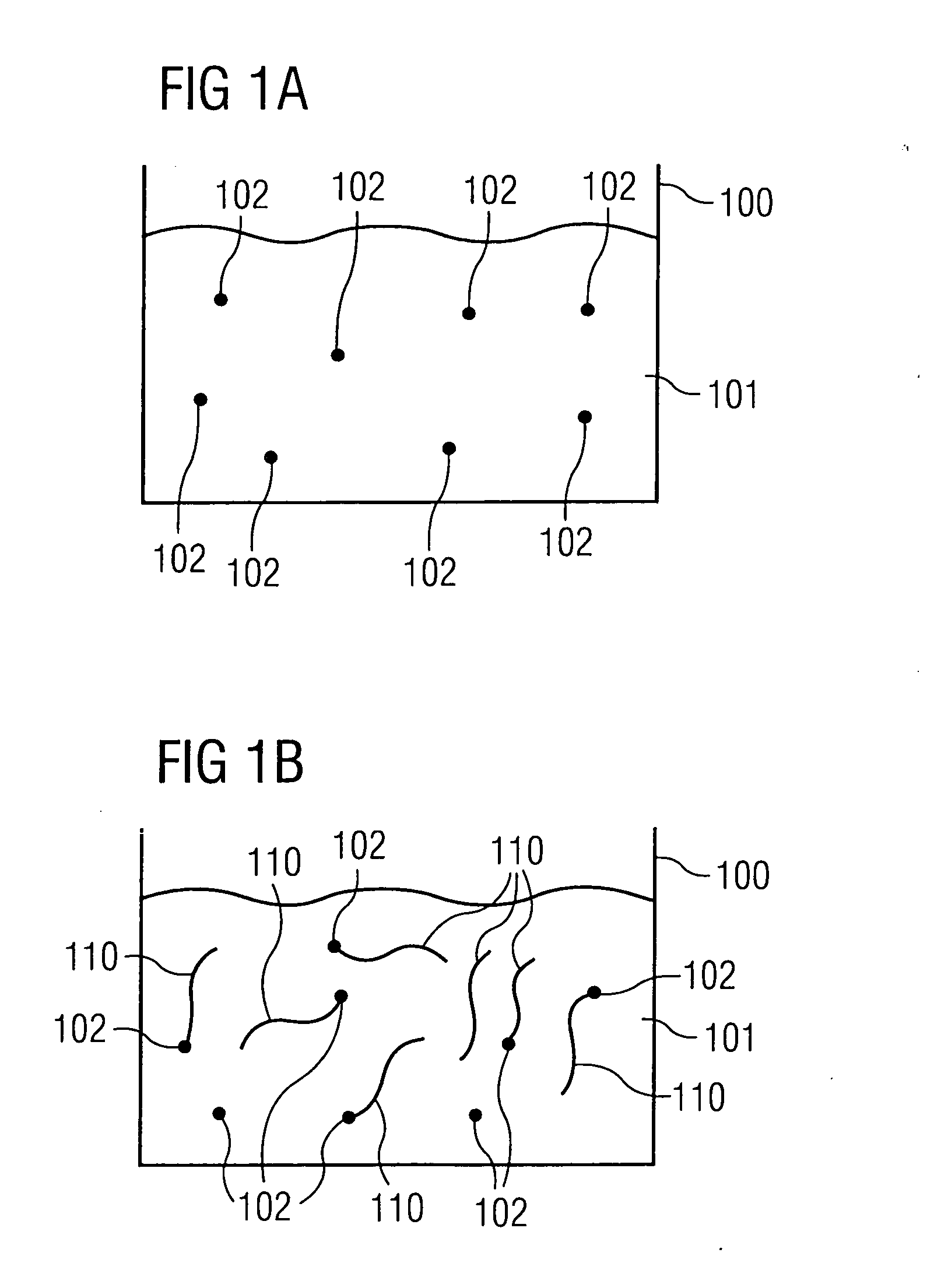
[0057]FIG. 1A shows a container 100 which contains a suspension of toluene solvent 101 and iron clusters 102. The iron clusters are surrounded by a thin film of oleic acid (not shown).

[0058]FIG. 1B shows the operating state of the container 100 after carbon nanotubes 110 have been introduced into the suspension using a CVD process. The carbon nanotubes 110 are surrounded along most of their length with a protective layer (not shown) of a photoresist, and the carbon nanotubes 110 are only free of the protective layer in a region surrounding an end section of the carbon nanotubes 110. After the carbon nanotubes 110 partially covered with the protective layer have been introduced into the suspension of toluene 101 and iron clusters 102, iron clusters 102 attach themse...


PUM


Abstract

The invention relates to a process for producing a nanoelement arrangement and to a nanoelement arrangement. In the process for producing a nanoelement arrangement, a first nanoelement is at least partially covered with catalyst material for catalyzing the growth of nanoelements. Furthermore, at least one second nanoelement is grown on the catalyst material.

Description

CROSS-REFERENCE TO RELATED APPLICATION [0001] This application is based on German Application No. 102 52 607.9, which was filed on Nov. 12, 2002. FIELD OF THE INVENTION [0002] The invention relates to a process for producing a nanoelement arrangement and to a nanoelement arrangement. BACKGROUND OF THE INVENTION [0003] With ongoing miniaturization, conventional silicon microelectronics will reach its limit. Disruptive short-channel effects are becoming an ever more important factor with ongoing miniaturization in a field-effect transistor, restricting the conductivity of the field-effect transistor. In addition to the problems which arise in an individual component, a further difficulty in a memory arrangement is a limited scaleability of the storage medium, for example the capacitance in a DRAM (dynamic random access memory) cannot be scaled to any desired degree. [0004] The use of carbon nanotubes is under discussion as a possible successor technology to silicon microelectronics. B...

Claims


Application Information

Patent Timeline
IPC IPC(8): H01L51/30
CPCB82Y10/00Y10S438/903Y10S977/891H01L51/0048H10K85/221
Inventor UNGER, EUGENDUSBERG, GEORG STEFANGRAHAM, ANDREWLIEBAU, MAIK
Owner POLARIS INNOVATIONS
Why Eureka
Try Eureka