

High transmittance overcoat for microlens arrays in semiconductor color imagers
a technology of color imagers and microlens arrays, which is applied in the field of optical design and microelectronics to achieve the effects of high transmittance, improved flexibility of design and layout of semiconductor array color imaging devices, and improved focus performan
- Summary
- Abstract
- Description
- Claims
- Application Information
AI Technical Summary
Benefits of technology
Problems solved by technology
Method used
Image

Examples
Embodiment Construction
The present invention discloses a simple fabrication sequence and the specific optical conditions and materials properties to be satisfied in forming an overcoat of high transmittance material to optimize long focal length microlens arrays for integrated semiconductor array color imaging devices.
Process Flow
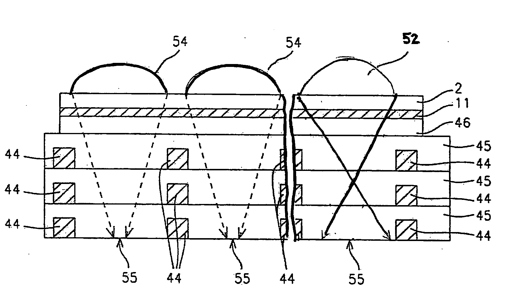
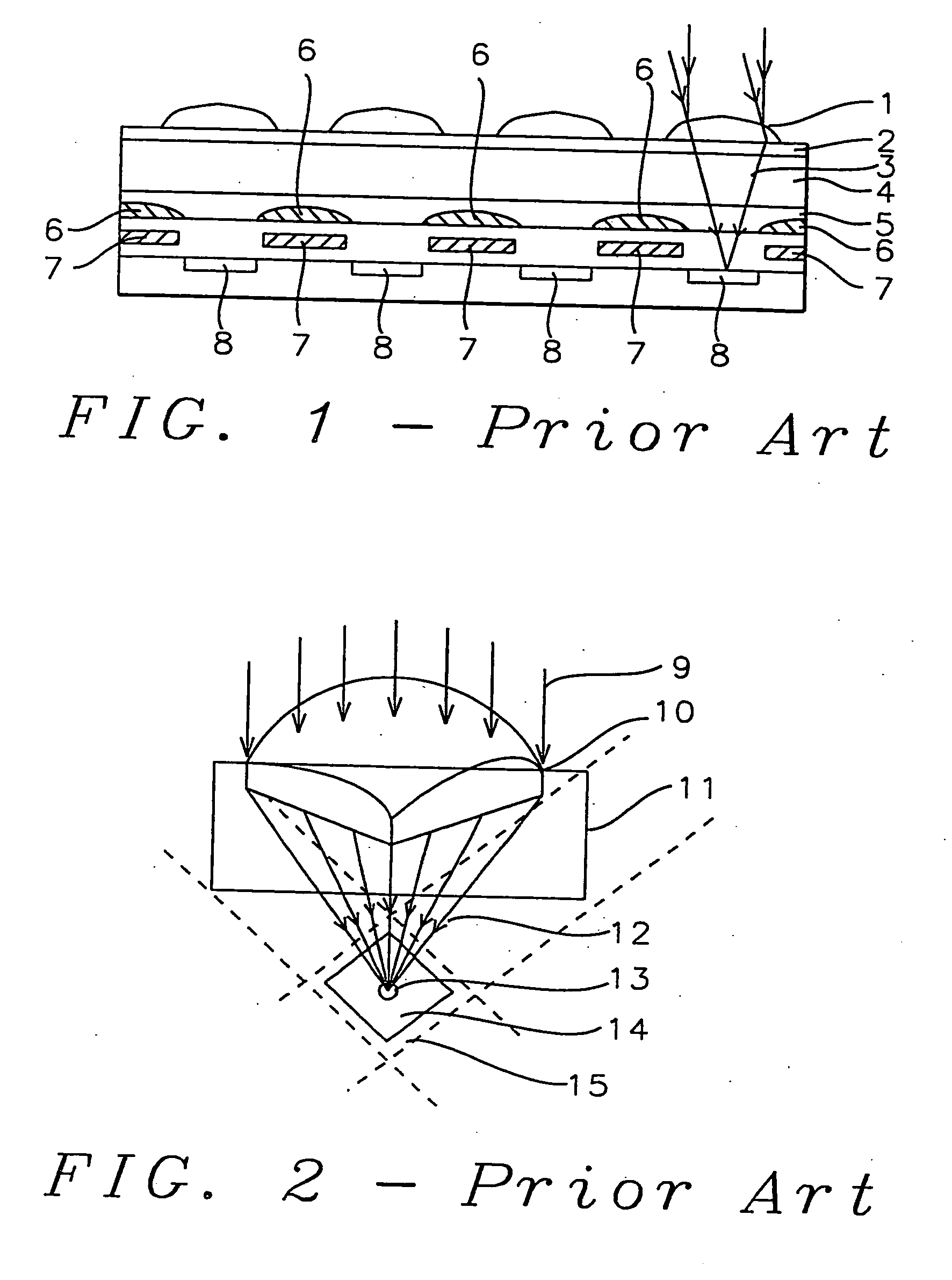
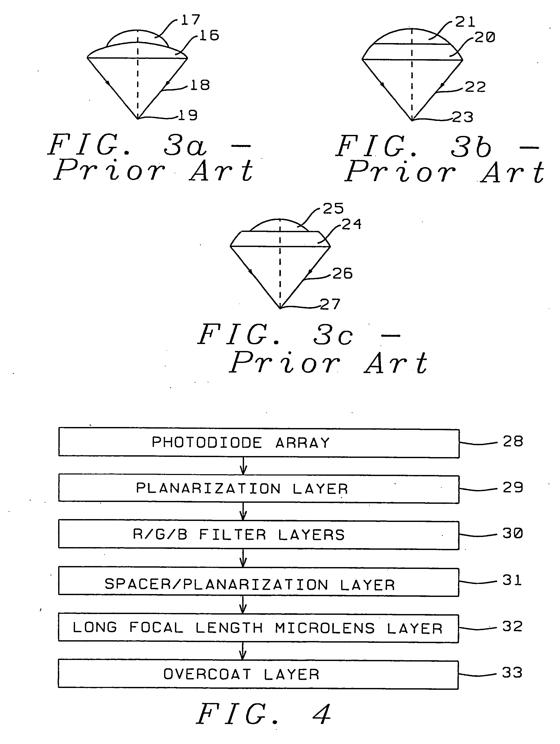
FIG. 4 depicts the simplified fabrication flow-chart of the process of the present invention, ordered in steps 28 through 33. In step 28 an array of image circuits having photosensitive areas are provided on a semiconductor substrate. In step 29 the array is coated with a transparent layer for passivation purposes which is planarized to accept the fabrication of an optical structure. This layer includes the necessary light shielding layers each with a planarization layer. In step 30 color filter layers are formed. In the preferred embodiment, three color layers are formed as detailed in FIG. 12. In step 31 another planarization (spacer) layer is formed which provides a level s...
PUM
 Abstract
Description
Claims
Application Information