Phase-changing sacrificial materials for manufacture of high-performance polymeric capillary microchips

a polymeric capillary microchip and phase-changing sacrificial material technology, applied in the direction of diaphragms, cells, optical parts, etc., can solve the problems of weak adhesion, complex and time-consuming fabrication process, and high cost of thermal bonding, so as to enhance the microchip analysis of biomolecules and improve protein focusing performan

Inactive Publication Date: 2012-01-24
WOOLLEY ADAM T +2
View PDF9 Cites 3 Cited by
  • Summary
  • Abstract
  • Description
  • Claims
  • Application Information

AI Technical Summary

Benefits of technology

[0021]Exemplary solvent bonded substrates have been made that can withstand internal pressures >2250 psi, much higher than thermally bonded PMMA made by prior-art processes. These solvent bonded substrates have demonstrated functionality as microfluidic systems performing rapid and high-resolution microchip capillary electrophoresis (CE) separations of fluorescently labeled amino acids and peptides. These separations compare favorably with glass microchip CE of peptide mixtures,26-28 and surpass those previously done on polymer microchips29-32 in terms of both speed and efficiency. Amino acid and peptide mixtures were separated in <15 s, with >40,000 theoretical plates in a 2.5 cm separation distance. Separations have been performed in electric fields as high as 1500 V / cm, the highest reported to date for polymer microchips. Finally, a single device was used for more than 300 runs over a three-month period without a decrease in separation performance, demonstrating long device lifetimes.
[0022]In general, solvent bonding is an appealing alternative to conventional thermal bonding techniques. Also known as solvent welding or solvent cementing, solvent bonding is a simple and economic method used commercially for joining polymeric materials. When a solvent is applied to the plastic, it softens and partially dissolves the substrate surfaces, allowing the polymer chains increased freedom of movement. If two solvent-softened pieces are then brought together under pressure, the material flows, and van der Waals attractive forces occur between the polymer chains in each substrate, which intermingle and diffuse into one another, such that after the solvent evaporates from the joined area, the two pieces remain sealed together.59 Unlike thermal bonding, solvent welding can be performed at or near room temperature, better preserving channel and surface integrity, while still allowing uniform composition of the device. Also, solvent bonding should allow facile surface modification prior to channel enclosure. Such functionalization may control electroosmotic flow and analyte adsorption, or provide attached chemical or biological groups on microchannel walls. In addition, the ability to construct microchip CE systems from different polymer substrates using simple room temperature bonding should increase the range of devices available for microfluidic experimentation.
[0033]The microchip EFGF devices according to the invention have offered improved protein focusing performance compared with capillary-based systems. In addition, these EFGF microchips can separate peptide samples with resolution similar to what is obtained in capillary electrophoresis microdevices, and the micro-EFGF systems enrich analytes by a factor of >150. Finally, hydrogel-integrated microfluidic devices have been fabricated that can concentrate protein samples over 10,000-fold. Interfacing microchannels with ion-permeable membranes has great potential to enhance microchip analysis of biomolecules.

Problems solved by technology

Despite these advantages, there are also several significant drawbacks to working with glass.
Expenses also accumulate during the many steps involved in preparing glass substrates, such as cleaning, photoresist coating, photolithography, development, etching, etc., making the fabrication process not only pricey, but also complicated and time consuming.
Unfortunately, glass microchips must be patterned and etched individually in a cleanroom, and the thermal annealing of glass substrates to enclose microcapillaries generally takes place in a furnace at >400° C. for several hours.1 Moreover, special care must be taken to ensure that the bonded surfaces are extremely clean and lacking even small particulates, or thermal bonding will not be successful.11 Low- and room-temperature glass bonding approaches that avoid high-temperature processing have been reported,12-15 but the resulting adhesion is weaker than in thermally sealed devices, and even greater care must be taken to ensure that the surfaces are extremely clean and flat.
While these sacrificial methods have successfully created devices without a thermal bonding step, the fabrication protocols are involved, and templated procedures are not possible because each device is patterned individually.
Since substances have characteristic surface charge distributions (or zeta potential), when a channel is comprised of different top and bottom materials, as is necessitated by adhesive and elastomer bonding, the different surface properties result in unwanted band broadening in separations.
On the other hand, the temperatures necessary for thermal bonding, normally >100° C. for polymers, often result in undesired reactions of microchip surface coatings.
For example, microfluidic mixers and reactors have been combined on microchip capillary electrophoresis (μ-CE) devices having six parallel separation lanes to perform multiple immunoassays in ˜1 min.80 In another case μ-CE systems with polymerase chain reaction chambers having on-chip heaters, temperature sensors and valves facilitated genotyping from whole bacterial cells in 81 However, one challenge associated with μ-CE is concentration sensitivity, since small sample volumes are loaded in these systems typically.
Such configurations have limited device geometries and are constrained by the properties of available materials.
Membrane properties could be altered by tailoring the prepolymer composition, but a complicated optical setup was required, and repeated laser exposures with fresh monomer solution in the channels were necessary to complete polymerization.
Although this approach allowed for smaller-dimension devices than previous membrane-incorporating EFGF designs,91-93,97 several limitations were also apparent.
For example, further column miniaturization was impractical, as thinner wires were more fragile and difficult to use.
In addition, a diameter mismatch between the focusing channel and the capillaries would reduce resolution if analytes were eluted from the column.

Method used


Image

  • Phase-changing sacrificial materials for manufacture of high-performance polymeric capillary microchips
  • Phase-changing sacrificial materials for manufacture of high-performance polymeric capillary microchips
  • Phase-changing sacrificial materials for manufacture of high-performance polymeric capillary microchips

Examples


example 1

Micro Fabrication

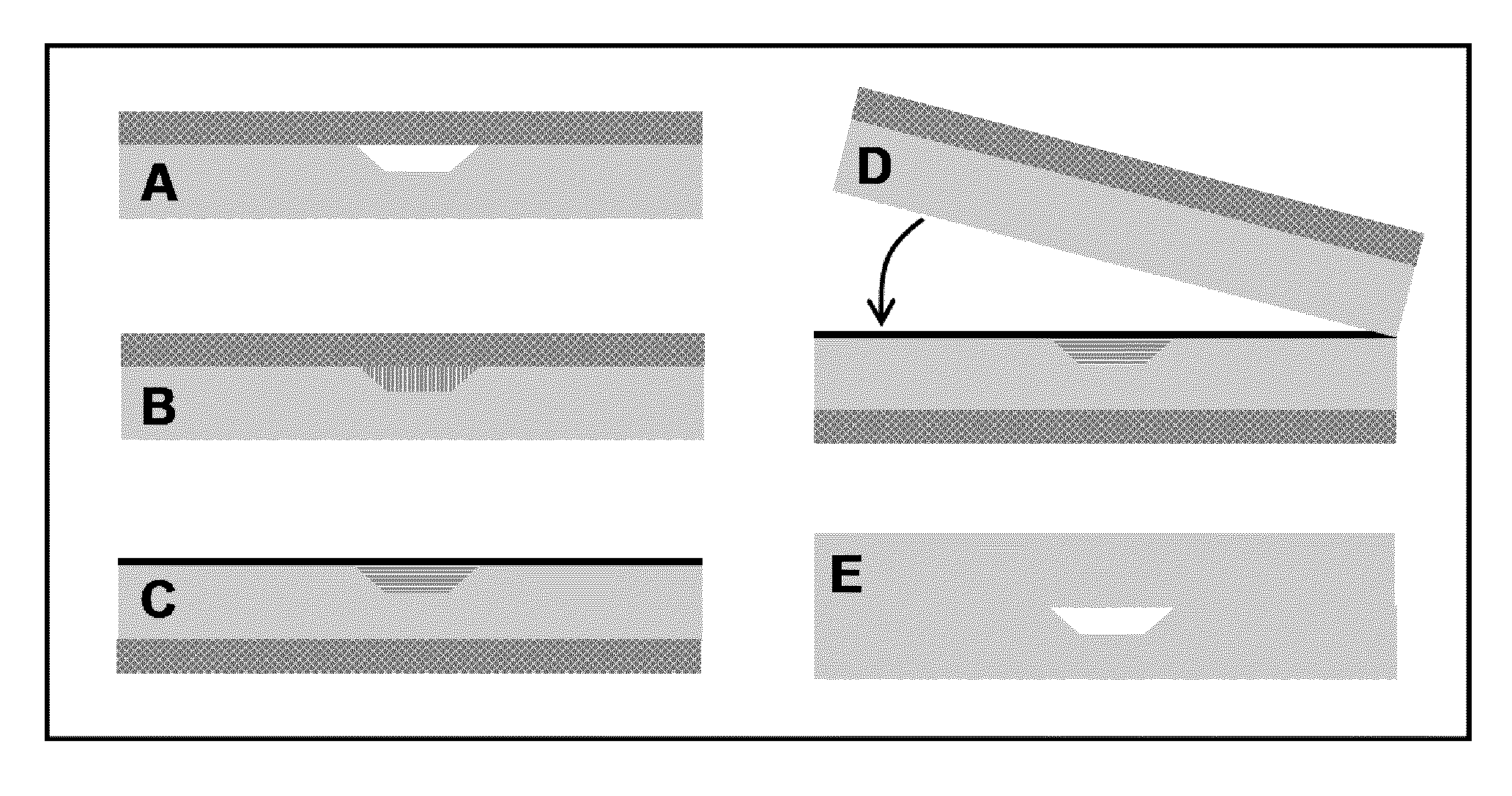
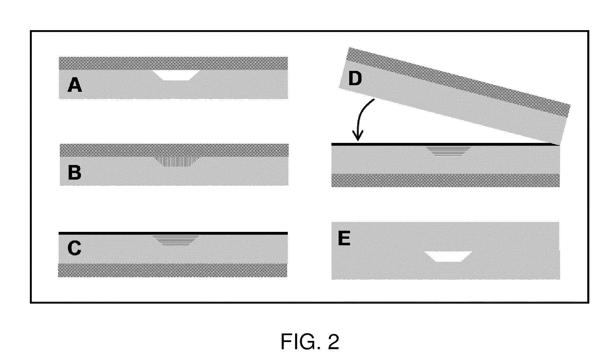
[0061]Reference is now made to FIG. 2. Microchips were made by imprinting raised features from photolithographically patterned and anisotropically etched silicon templates into PMMA substrates using previously described methods.33 Imprinted PMMA substrates (Acrylite OP-3, Cyro, Rockaway, N.J.) were 1.75″×1″×⅛″ and had 3-mm-diameter reservoir holes aligned with the channel ends. A CO2 laser cutter (C-200, Universal Laser Systems, Scottsdale, Ariz.) was used to excise the PMMA substrates from larger sheets and create the reservoir holes. A clean, flat, 1 / 16″-thick piece of PDMS (Sylgard 184, Dow Corning, Midland, Mich.), which had been cured according to the manufacturer's specifications, was sealed to the patterned side of a PMMA substrate (FIG. 2A), temporarily forming enclosed channels. The PMMA / PDMS assembly was mounted on a glass microscope slide and placed on a heating block at 85° C. (above the melting temperature of the paraffin wax) for 30 s. A pipet was used...

example i

Conclusion and Summary of Example I

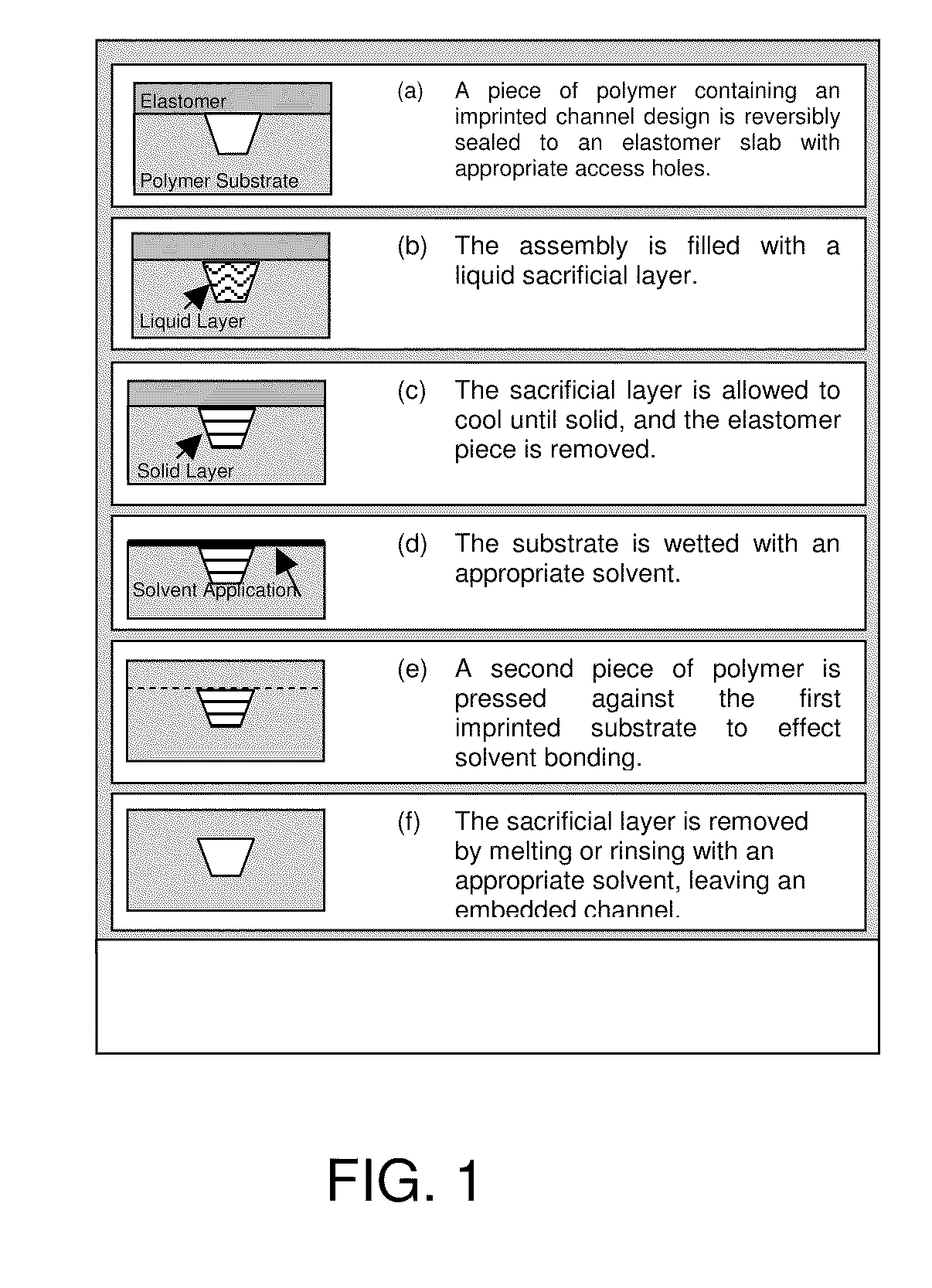
[0075]It has been shown that polymeric microchips can be created by using a sacrificial material to protect channel integrity during solvent bonding. This phase-changing sacrificial material fabrication method is simple to implement, and tests show that solvent-bonded devices can withstand >10-fold higher internal pressures than thermally bonded substrates. CE separations of FITC-labeled amino acids and peptides were successfully carried out on solvent-bonded devices in as little as 8 and 15 s, respectively, with theoretical plate numbers exceeding 40,000 for both analyses. Finally, devices can be operated at electric fields >1500 V / cm and can be used for hundreds of electrophoretic separations without any change in performance. Solvent bonding with phase-changing sacrificial materials should help to overcome some of the previous limitations of polymer microfluidic devices and make them more attractive for chemical analyses.

Example II

Imprinting

[007...

example ii

Conclusions and Summary of Example II

[0105]Solvent bonding of PC and PETg has been demonstrated as a realistic option for fabrication of CE microchips. Thermal imprinting techniques for these two polymers were developed, and solvent embossing was explored as an alternative. Different bonding solvents and phase-changing sacrificial materials were also evaluated, and the best results were obtained with acetonitrile as the solvent and Crème wax as the sacrificial material. Finally, simple CE separations were performed on completed devices to assess their potential for microchip chemical analysis applications. The fabrication techniques developed and implemented here have the potential to both simplify and improve microdevice construction.

Example III

Sample Preparation and Materials

[0106]All buffer solutions were made using purified water from a Barnstead EasyPure UV / UF system (Dubuque, Iowa) and passed through a 0.2-μm filter (Pall, East Hills, N.Y.) prior to use. Peptide standards (Sig...


PUM

PropertyMeasurementUnit
temperatureaaaaaaaaaa
diametersaaaaaaaaaa
temperaturesaaaaaaaaaa

Abstract

A microchip with capillaries and method for making same is described. A sacrificial material fills microchannels formed in a polymeric substrate, the filled microchannels are covered by a top cover to form filed capillaries, and the sacrificial material is removed to form the microcapillaries. The sacrificial material fills the microchannels as a liquid whereupon it becomes solid in the microchannels, and is liquefied after the top cover is applied and affixed to remove the sacrificial material. The top cover may be solvent sealed on the substrate and of the same or different material as the substrate. The top cover may also be an in situ applied semipermeable membrane.

Description

CROSS REFERENCE TO RELATED APPLICATIONS[0001]This application is a divisional from U.S. patent application Ser. No. 11 / 346,398, filed 1 Feb. 2006 now U.S. Pat. No. 7,686,907, which claims priority from U.S. Provisional Patent Application 60 / 649,325, filed 1 Feb. 2005.FEDERAL RESEARCH STATEMENT[0002]This invention was made with support from United States Government, and the United States Government has certain rights in this invention pursuant to contract number R01 GM064547-01 A1, National Institutes of Health.BACKGROUND OF INVENTION[0003]Although a relatively new area of study, micromachined chemical analysis systems have the potential to revolutionize separation methods, much like integrated circuit manufacturing transformed advanced computation in the twentieth century. Miniaturized devices promise to reduce both reagent consumption and cost while simultaneously increasing separation speed and throughput. Already, microdevices have been utilized in clinical diagnostics41, analyti...

Claims


Application Information

Patent Timeline
Patent Type & Authority Patents(United States)
IPC IPC(8): B32B17/00C03C27/00B32B17/10C03C15/00G01N15/06G01N33/00C03C25/68G02C7/00B29C53/82G01N21/00G01N31/22
CPCB01L3/502707B29C65/4895B29C65/76B29C66/022B29C66/032B29C66/3242B32B37/0023B32B38/06B81C1/00071B29C66/53461B01L2200/0689B01L2300/0816B01L2300/0887B29C66/0224B29C66/0246B29K2021/00B29K2033/12B29K2067/00B29K2067/043B29K2069/00B29K2083/00B29L2031/756B32B2309/027B32B2323/16B32B2333/12B32B2367/00B32B2369/00B81B2201/058B81C2201/0108B81C2203/038G01N21/05G01N2021/0346G01N2021/6439B29C65/00G01N27/44791B29C66/026B29C66/71B29C66/73117B29C66/1122B29K2067/003
Inventor WOOLLEY, ADAM T.KELLY, RYAN T.FISK, MELISSA DRAPER
Owner WOOLLEY ADAM T
Why Eureka
Try Eureka