Thin film transistor and multilayer film structure and manufacturing method of same

Inactive Publication Date: 2005-03-03
VIDEOCON GLOBAL
View PDF3 Cites 16 Cited by
  • Summary
  • Abstract
  • Description
  • Claims
  • Application Information

AI Technical Summary

Benefits of technology

[0016] Preferably, the insulating layer is patterned by plating a sacrificial layer on the second metal layer and subjecting the structure to an etchant that etches the insulating film and removes the sacrificial layer, thereby forming an offset region in the insulating film that extends beyond the dimensions of the second metal layer. Using plating to form the sacrificial layer enables the offset regions to be uniform (substan

Problems solved by technology

However, since the conventional 7 PEP structure requires a number of steps and the process itself becomes complex, manufacturing cost

Method used


Image

  • Thin film transistor and multilayer film structure and manufacturing method of same
  • Thin film transistor and multilayer film structure and manufacturing method of same
  • Thin film transistor and multilayer film structure and manufacturing method of same

Examples


embodiment 1

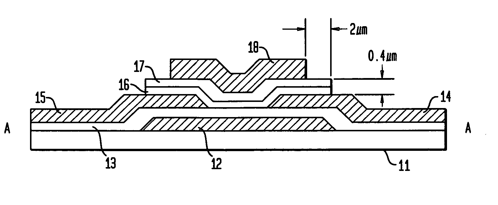
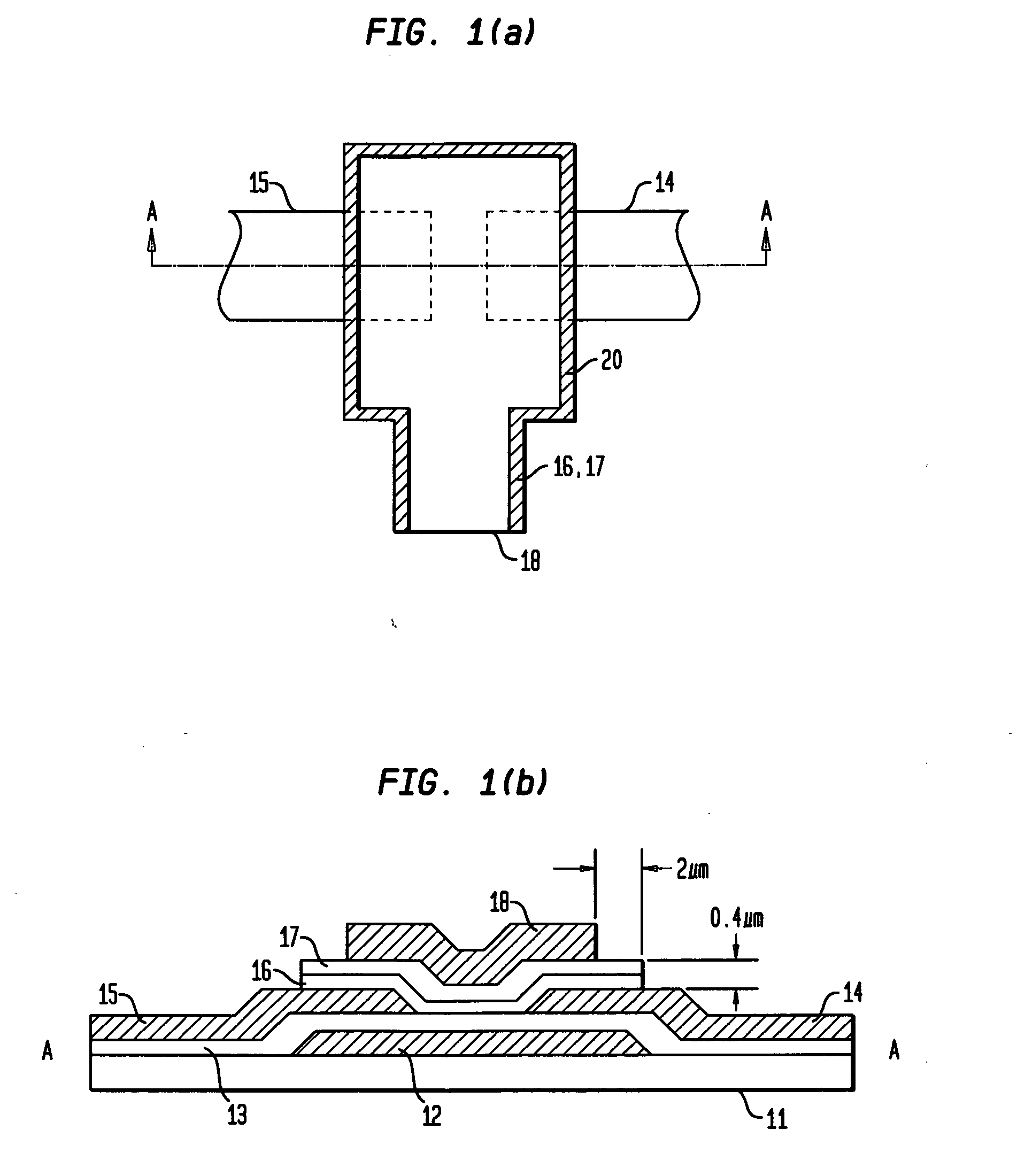
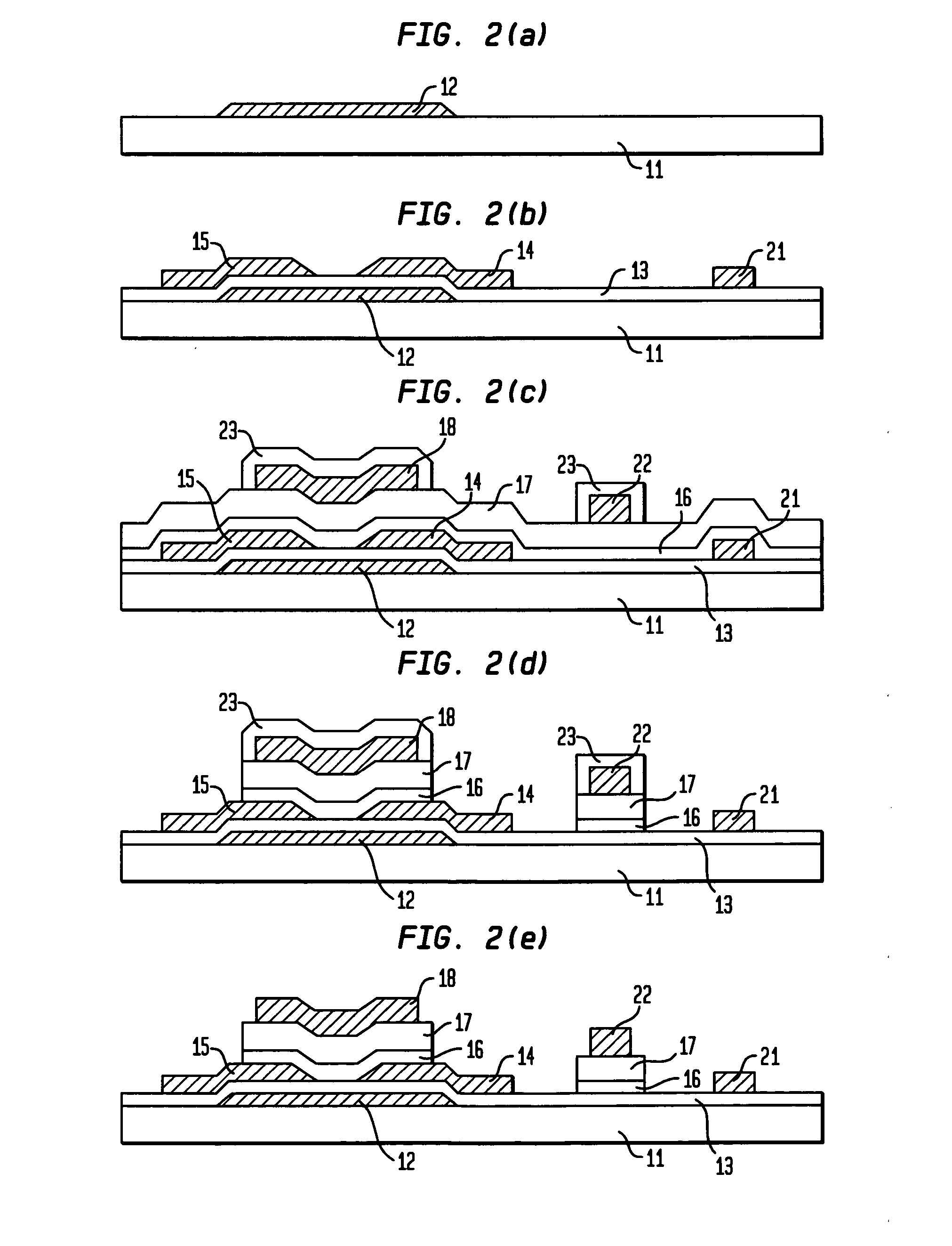
[0024] Each of FIGS. 1(a) and 1(b) is a view showing a thin film transistor (TFT) structure of the present invention, by taking an example of a TFT of a top gate type. Specifically, FIG. 1(a) shows a state of the TFT when seen from above, which is manufactured in a shortened process by a later-described manufacturing method; and FIG. 1(b) shows an A-A section of FIG. 1(a).

[0025] As shown in FIG. 1(b), the TFT of the embodiment comprises a light shielding film (light shield) 12 formed on an insulating substrate 11 made of no-alkali glass, quartz or the like, and an insulating film 13 formed as an undercoated layer to cover the upper portion thereof, the undercoated layer being made of an oxidized silicon nitride film SiOxNy or the like. Preferably, the light shielding film 12 is formed by printing-and-plating copper (CU). On the insulating film 13, source and drain electrodes 14 and 15 are formed. Preferably, the source and drain electrodes are formed by printing-and-plating cobalt (...

second embodiment

[0039] The description above illustrates an embodiment of the present invention in a TFT of a top gate type. Next, description will be made for the present invention in a TFT of a bottom gate type and another multilayer film structure, to which the present invention is applied.

[0040] Each of FIGS. 3(a) and 3(b) is a view illustrating a constitution of this second embodiment. FIG. 3 (a) shows the state where the gate electrode 31 and the data line 32 cross to each other. FIG. 3(b) shows a B-B section of FIG. 3(a). In the multilayer film structure of the embodiment, as shown in FIG. 3(b), an a-Si film 34 and a gate insulating film 35 are formed on a gate electrode 31, and a data line 32 is formed on the gate insulating film 35. If an end surface of the data line 32 coincides with an etching end surface of the a-Si film 34 or the gate insulating film 35, then a short circuit may occur between the gate electrode 31 and the data line 32 at a crossing position like that shown in FIG. 3(a)...


PUM


Abstract

The present invention is directed to a thin film transistor (and related multilayer structures) that includes: source and drain electrodes 14 and 15 disposed at a specified interval above an insulating substrate 11 and formed by printing-and-plating; an a-Si film 16 disposed for the source and drain electrodes 14 and 15; a gate insulating film 17 laminated on the a-Si film 16; and a gate electrode 18 laminated on the gate insulating film 17 and formed by printing-and-plating. The a-Si film 16 and the gate insulating film 17 have an offset region 20 that uniformly extends beyond the dimensions of the gate electrode 18.

Description

BACKGROUND OF THE INVENTION [0001] The present invention relates to a thin film transistor used for a liquid crystal display of an active matrix system or the like. The invention also relates to methods for manufacturing a multilayer film structure and the thin film transistor. [0002] The liquid crystal display of an active matrix system that uses a thin film transistor is constructed in a manner that a gate electrode (Y electrode) and a data electrode (X electrode) are disposed in a matrix form, and a liquid crystal is sealed in between a TFT array substrate having a thin film transistor (TFT) disposed at an intersection thereof and an opposite substrate laminated by keeping a gap with the TFT array substrate. The liquid crystal display can perform displaying by using the thin film transistor to control a voltage applied to the liquid crystal, and also by using an electro-optical effect provided by the liquid crystal. [0003] Conventionally known thin film transistor structures incl...

Claims


Application Information

Patent Timeline
IPC IPC(8): G02F1/1335G02F1/1362G02F1/1368H01L21/288H01L21/3205H01L21/336H01L21/77H01L21/84H01L27/12H01L29/417H01L29/786
CPCH01L27/12H01L29/41733H01L29/66757H01L27/1292H01L29/78633H01L29/78666H01L29/78696H01L29/78609H01L29/786
Inventor FRYER, PETER M.WISNIEFF, ROBERT L.TSUJIMURA, TAKATOSHI
Owner VIDEOCON GLOBAL
Why Eureka
Try Eureka