Plated terminations

a technology of multi-layer electronic components and termination stripes, which is applied in the direction of fixed capacitor electrodes, metallic pattern materials, solid-state devices, etc., can solve the problems of reduced chip size, difficult to print termination stripes in a predetermined area with required precision, and difficult control of termination stripes application, etc., to eliminate or greatly simplify thick-film stripes. , the effect of improving the termination featur

Inactive Publication Date: 2005-03-03
KYOCERA AVX COMPONENTS CORP
View PDF100 Cites 143 Cited by
  • Summary
  • Abstract
  • Description
  • Claims
  • Application Information

AI Technical Summary

Benefits of technology

[0012] The present subject matter recognizes and addresses various of the foregoing shortcomings, and others concerning certain aspects of electrical terminations and related technology. Thus, broadly speaking, a principal object of the presently disclosed technology is improved termination features for electronic components. More particularly, the disclosed termination features are plated and designed to eliminate or greatly simplify thick-film stripes that are typically printed along portions of a monolithic device for termination purposes.

Problems solved by technology

The application of terminations is often hard to control and can become problematic with reduction in chip sizes.
The ever-shrinking size of electronic components makes it quite difficult to print termination stripes in a predetermined area with required precision.
Reduced component size or an increased number of termination contacts for an electronic chip device may cause the resolution limits of typical termination machines to become maxed out.
Other problems that can arise when trying to apply selective terminations include shifting of the termination lands, mispositioning of terminations such that internal electrode tabs are exposed or missed entirely, and missing wrap-around termination portions.
Yet further problems may be caused when too thin a coating of the paint-like termination material is applied or when one portion of termination coating smears into another causing shorted termination lands.
While various aspects and alternative features are known in the field of electronic components and terminations therefor, no one design has emerged that generally addresses all of the issues as discussed herein.

Method used


Image

  • Plated terminations
  • Plated terminations
  • Plated terminations

Examples


embodiment 16

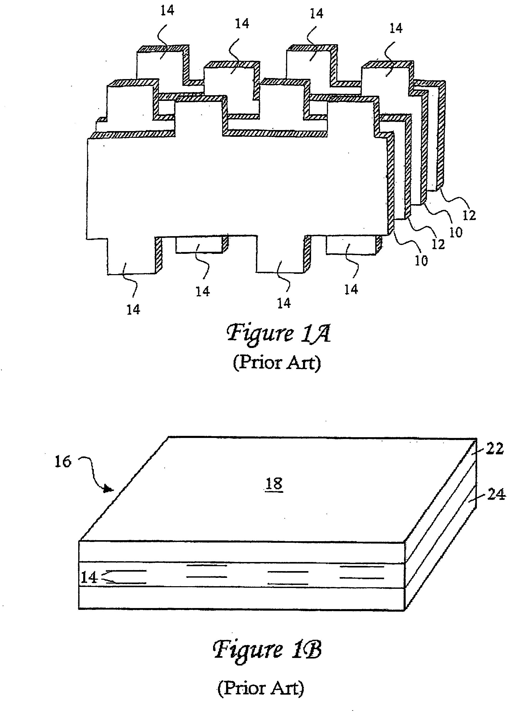
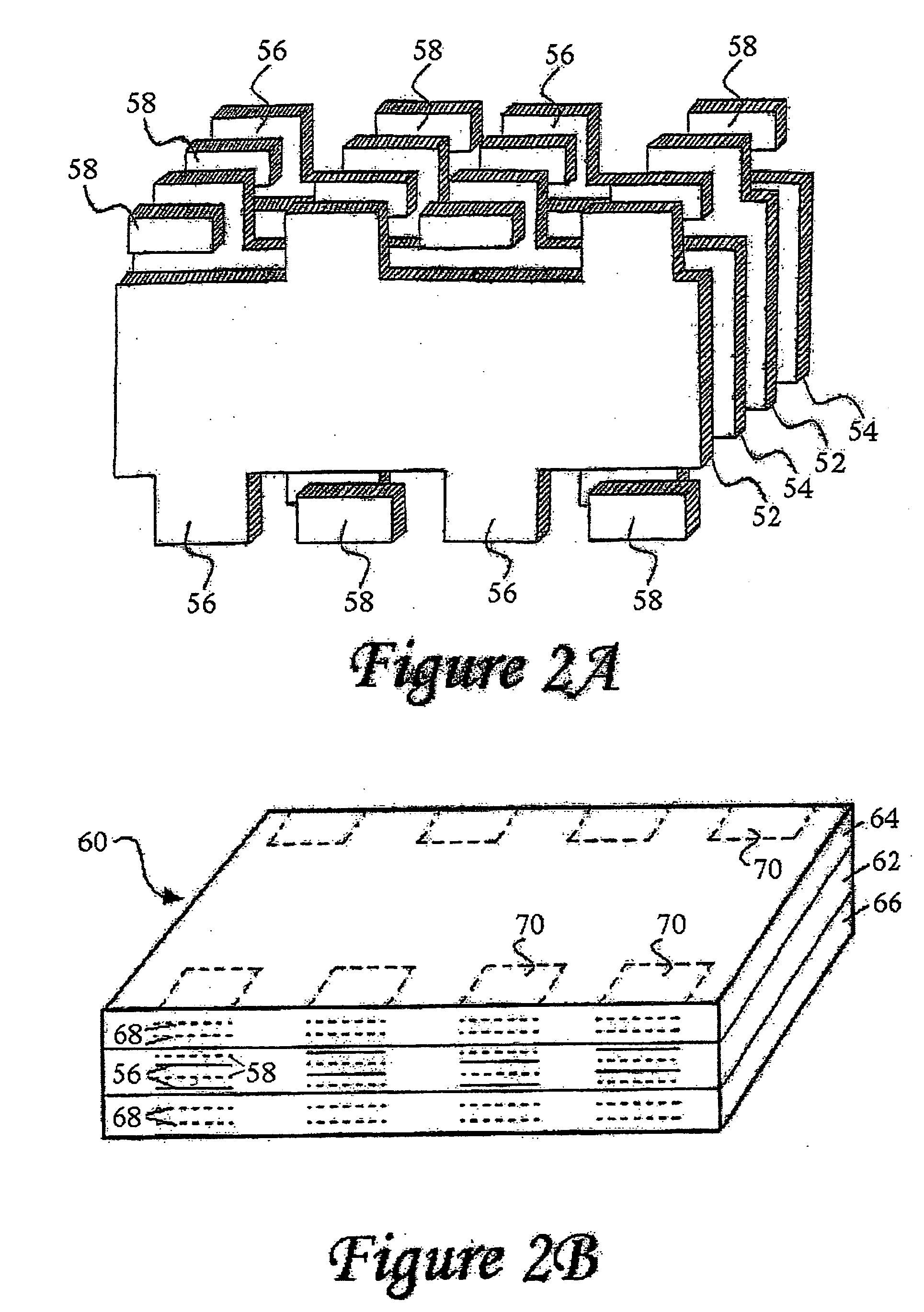
[0057] An interdigitated capacitor typically consists of a plurality of electrode layers, such as those shown in FIG. 1A disposed in a body of dielectric material 18, such as seen in the exemplary interdigitated capacitor configuration 16 of FIG. 1B. Electrode layers 10 and 12 are disposed in the dielectric material 18 such that electrode tabs 14 extend to and are exposed at two sides of IDC embodiment 16. Exemplary materials for such electrode layers may include platinum, nickel, a palladium-silver alloy, or other suitable conductive substances. Dielectric material 18 may comprise barium titanate, zinc oxide, alumina with low-fire glass, or other suitable ceramic or glass-bonded materials. Alternatively, the dielectric may be an organic compound such as an epoxy (with or without ceramic mixed in, with or without fiberglass), popular as circuit board materials, or other plastics common as dielectrics. In these cases the conductor is usually a copper foil which is chemically etched t...

embodiment 74

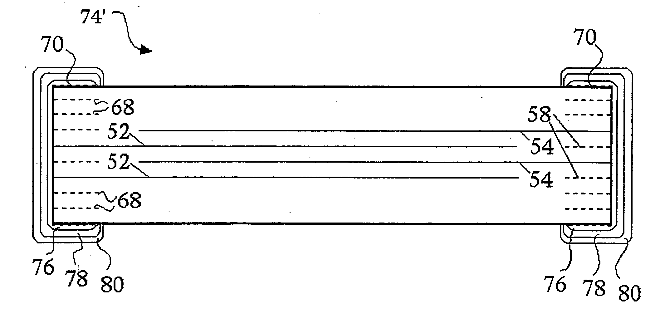
[0072] There are several different techniques that can potentially be used to form plated terminations, such as terminations 72 on multilayer component embodiment 74 of FIG. 8A. As previously addressed, a first method corresponds to electroplating or electrochemical deposition, wherein an electronic component with exposed conductive portions is exposed to a plating solution such as electrolytic nickel or electrolytic tin characterized by an electrical bias. The component itself is then biased to a polarity opposite that of the plating solution, and conductive elements in the plating solution are attracted to the exposed metallization of the component. Such a plating technique with no polar biasing is referred to as electroless plating, and can be employed in conjunction with electroless plating solutions such as nickel or copper ionic solution.

[0073] In accordance with electrochemical deposition and electroless plating techniques, a component such as IDC 74 of FIG. 8A, is preferably...


PUM

PropertyMeasurementUnit
thicknessaaaaaaaaaa
thicknessaaaaaaaaaa
sizeaaaaaaaaaa

Abstract

Improved termination features for multilayer electronic components are disclosed. Monolithic components are provided with plated terminations whereby the need for typical thick-film termination stripes is eliminated or greatly simplified. Such termination technology eliminates many typical termination problems and enables a higher number of terminations with finer pitch, which may be especially beneficial on smaller electronic components. The subject plated terminations are guided and anchored by exposed internal electrode tabs and additional anchor tab portions which may optionally extend to the cover layers of a multilayer component. Such anchor tabs may be positioned internally or externally relative to a chip structure to nucleate additional metallized plating material. External anchor tabs positioned on top and bottom sides of a monolithic structure can facilitate the formation of wrap-around plated terminations. The disclosed technology may be utilized with a plurality of monolithic multilayer components, including interdigitated capacitors, multilayer capacitor arrays, and integrated passive components. A variety of different plating techniques and termination materials may be employed in the formation of the subject self-determining plated terminations.

Description

PRIORITY CLAIM [0001] This application claims the benefit of previously filed U.S. Provisional Patent Application entitled “PLATED TERMINATIONS,” assigned U.S. Ser. No. 60 / 372,673, filed Apr. 15, 2002, and which is incorporated herein by reference for all purposes.BACKGROUND OF THE INVENTION [0002] The present subject matter generally concerns improved termination features for multilayer electronic components, and more particularly relates to plated terminations for multilayer capacitors or integrated passive components. The subject termination design utilizes selective arrangements of internal and / or external electrode tabs to facilitate the formation of plated electrical connections. The external connections are preferably made whereby the provision of typical thick film termination stripes is eliminated or greatly simplified. [0003] Many modern electronic components are packaged as monolithic devices, and may comprise a single component or multiple components within a single chip...

Claims


Application Information

Patent Timeline
Patent Type & Authority Applications(United States)
IPC IPC(8): B05D5/12H01F5/00H01G4/252H01G4/005H01G4/228H01G4/30H01G7/00H01L23/48H05K1/09H05K1/11
CPCH01C1/14Y10T29/49099H01C7/10H01G4/005H01G4/012H01G4/228H01G4/232H01G4/30H05K3/403H05K2201/09709C25D5/02H05K3/02Y10T29/42Y10T29/43Y10T29/49101Y10T29/435Y10T29/417Y10T29/49002H01C7/008C25D7/00C23C18/1651C23C18/1653C23C18/32C23C18/38C23C18/48C23C28/021C23C28/023H01G4/008H01G4/12C25D3/56C25D5/34H01C17/28H01F41/04H01G4/06
Inventor RITTER, ANDREW P.HEISTAND, ROBERT IIGALVAGNI, JOHN L.DATTAGURU, SRIRAM
Owner KYOCERA AVX COMPONENTS CORP
Why Eureka
Try Eureka