Method of etching magnetic material, magnetoresistive film and magnetic random access memory

a magnetic material and random access memory technology, applied in the field of etching a magnetic material, can solve the problems of difficult to prevent a removed substance from adhering to a workpiece, the element size cannot be reduced, and the recording density cannot be greatly improved

Active Publication Date: 2005-03-03
CANON KK
View PDF7 Cites 25 Cited by
  • Summary
  • Abstract
  • Description
  • Claims
  • Application Information

AI Technical Summary

Benefits of technology

[0015] To achieve the above-described object, a method of a magnetic material of the present invention is a method of etching a magnetic material which contains a rare earth metal and a transition metal as main component elements, which has the step of reducing a component ratio of the transition metal to the rare earth metal of a sidewall substance, which adheres to the magnetic material when the magnetic material is etched, to a value smaller than a component ratio of the transition metal to the rare earth metal in the magnetic material.

Problems solved by technology

However, when the element size is reduced in order to increase the recording density of MRAM, MRAM which uses an in-plane magnetized film cannot retain information due to the effects of a diamagnetic field or the curling of the magnetization of an end surface, thus posing a problem.
Under the method, however, the element size cannot be reduced and hence a great improvement in recording density cannot be expected.
However, in the etching of MRAM which uses a magnetoresistive film in which a magnetic film contains a substance having a higher melting point than Si, it is difficult to prevent a removed substance from adhering again to a workpiece.
In a magnetoresistive film in which a current is caused to flow in a direction perpendicular to the film plane, the first magnetic film and the second magnetic film short electrically due to the formation of a sidewall substance on a sidewall of the electromagnetic film, and it becomes impossible to obtain the magnetoresistive effect.
For this reason, also in this case, a current flowing via the sidewall substance increases similarly and it is feared that a sufficient magnetoresistive effect could not be obtained.

Method used


Image

  • Method of etching magnetic material, magnetoresistive film and magnetic random access memory
  • Method of etching magnetic material, magnetoresistive film and magnetic random access memory
  • Method of etching magnetic material, magnetoresistive film and magnetic random access memory

Examples


first embodiment

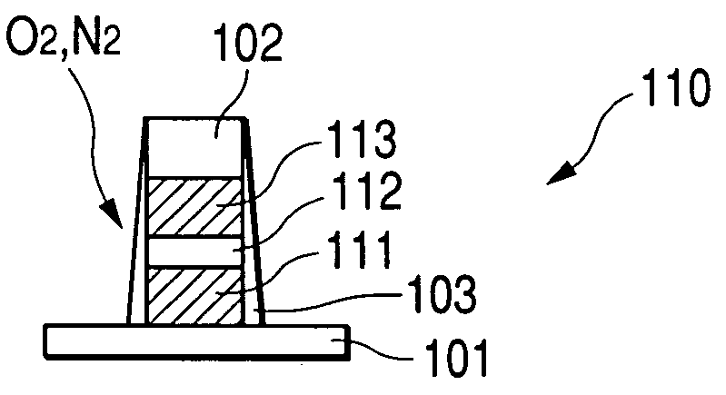
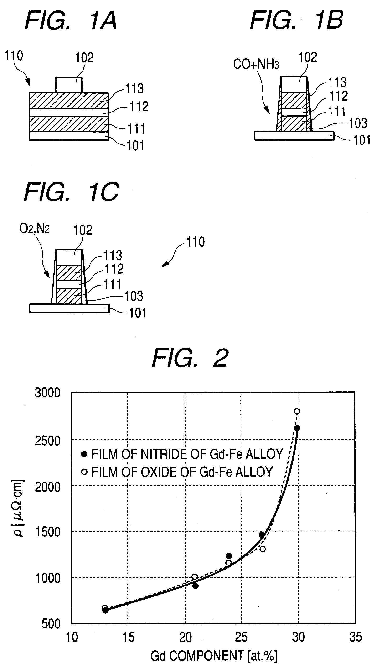
[0048] As shown in FIG. 1A, a perpendicular magnetized film of Gd20(Fe50Co50)80 was formed as a first magnetic film 111 by sputtering with a thickness of 10 nm on a substrate 101 formed from a Si wafer and an Al film was then continuously formed by sputtering with a thickness of 1.5 nm. After that, by the plasma oxidation of the Al film in an O2 atmosphere, an oxidized Al film was formed as a tunnel insulating film 112, which is an insulating film. Subsequently, a perpendicular magnetized film of Tb19(Fe50Co50)81 was formed, as a second magnetic film 113, with a thickness of 10 nm on the tunnel insulating film 112. Furthermore, a Pt film was formed, as a protective film (not shown), with a thickness of 5 nm on the second magnetic film 113.

[0049] Furthermore, a resist film 102 having a size of 180 nm×180 nm was formed on the TMR element 110 obtained as described above and the interior of a vacuum chamber (not shown) was evacuated, with this TMR element 110 held in the vacuum chamber...

second embodiment

[0051] In the same manner as in the first embodiment, a perpendicular magnetized film of Gd20(Fe50Co50)80 having a thickness of 10 nm as a first magnetic film 111, a tunnel insulating film 112 which is an insulating film formed from an oxidized Al film with a thickness of 1.5 nm, a perpendicular magnetized film of Tb19(Fe50Co50)81 with a thickness of 10 nm as a second magnetic film 113, and a Pt film with a thickness of 5 nm as a protective film (not shown) were sequentially formed on a substrate 101 formed from a Si wafer, and a TMR element of the same film structure as the first embodiment was formed.

[0052] Furthermore, a resist film 102 having a size of 180 nm×180 nm was formed on the TMR element 110 obtained as described above and the interior of a vacuum chamber (not shown) was evacuated, with this TMR element 110 held in the vacuum chamber. And a mixed gas of CO and NH3 was introduced into the vacuum chamber and the TMR element 110 was dry etched to the surface of the substra...

third embodiment

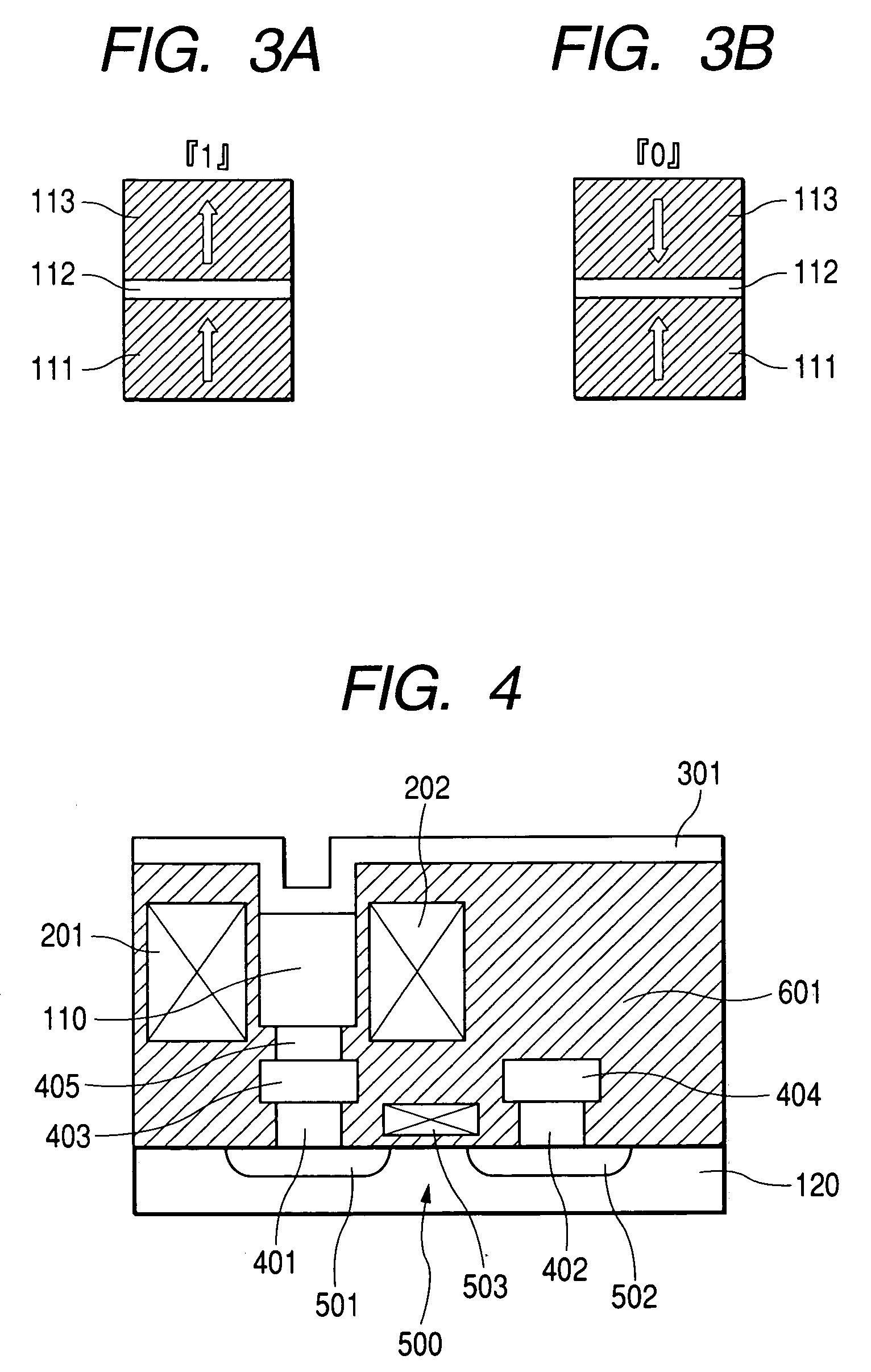
[0054] In this embodiment, a description will be given about an example in which MRAM uses a magnetoresistive film in which the composition ratio of a transition metal to a rare earth metal of a side wall substance formed on sidewalls of a magnetic layer and a nonmagnetic layer is smaller than the composition ratio of a transition metal to a rare earth metal in the magnetic layer. By correlating the magnetization direction of a magnetic film with “1” and “0” of digital information, it is possible to form a memory device from a TMR element.

[0055] As shown in FIGS. 3A and 3B, in a TMR element in which magnetic films 111, 113 are formed above and under a tunnel insulating film 112, which is an insulating film, to as to be in contact with the tunnel insulating film 112, the resistance value when the magnetization direction of a transition metal contained in the two magnetic films 111, 113 is the same as in FIG. 3A is small compared to a case where as shown in FIG. 3B, the magnetization...


PUM

PropertyMeasurementUnit
sizeaaaaaaaaaa
thicknessaaaaaaaaaa
electric resistivityaaaaaaaaaa

Abstract

Provided are a method of etching a magnetic material which enables a current flowing via a sidewall substance to be suppressed to a greater extent, and the like.
A spin tunneling magnetoresistive film 110, which comprises a first magnetic film 111, a tunnel film 112 and a second magnetic film 113, is formed on a substrate 101, and on the top surface of the spin tunneling magnetoresistive film 110 a resist film 102 having a desired shape is formed. The magnetic films 111, 113 are each an alloy film of a rare earth metal-transition metal. The spin tunneling magnetoresistive film 110 is plasma etched by using a mixed gas of carbon monoxide gas and ammonia gas. A sidewall substance 103 adhering to a side surface of the spin tunneling magnetoresistive film 110 is oxidized or nitrided by performing plasma etching by use of oxygen gas or nitrogen gas.

Description

BACKGROUND OF THE INVENTION [0001] 1. Field of the Invention [0002] The present invention relates to a method of etching a magnetic material and the like and, more particularly, to a method of etching a spin tunneling magnetoresistive film and the like. [0003] 2. Related Background Art [0004] In recent years, MRAM (Magnetic Random Access Memory) which is a high speed nonvolatile memory has been attracting attention as a memory which replaces many solid memories which are at present in use. In particular, MRAM which utilizes the spin tunneling magnetoresistive effect is favorable for high recording density design or high speed read because large read signals are obtained, and the possibility as MRAM has been demonstrated in recent study reports. [0005] The basic structure of a magnetoresistive film used as an element of MRAM is a sandwich structure in which magnetic layers are formed in an adjacent manner via a nonmagnetic layer. However, when the element size is reduced in order to ...

Claims


Application Information

Patent Timeline
Patent Type & Authority Applications(United States)
IPC IPC(8): G11C11/16G11C11/15H01F10/32H01F41/30H01L21/00H01L21/3065H01L21/3213H01L21/8239H01L21/8246H01L27/105H01L27/22H01L43/08H01L43/12
CPCB82Y25/00B82Y40/00H01F10/3254H01L43/12H01L21/32135H01L27/228H01F41/308H10B61/22H10N50/01
Inventor IKEDA, TAKASHI
Owner CANON KK
Why Eureka
Try Eureka