Semiconductor device and manufacturing method for the same

a semiconductor and semiconductor technology, applied in the field of semiconductor devices, can solve the problems of large drop in inability to improve the trade-off relationship between the main withstand voltage and the on resistance, and difficulty in implementation

Inactive Publication Date: 2005-03-03
MITSUBISHI ELECTRIC CORP
View PDF11 Cites 56 Cited by
  • Summary
  • Abstract
  • Description
  • Claims
  • Application Information

AI Technical Summary

Benefits of technology

[0041] An object of the present invention is to provide a structure which improves the trade-off relationship between the main withstanding voltage and the ON resistance, and a manufacturing method capable of implementing such a structure in a semiconductor device based on a three-dimensional multiple RESURF effect.

Problems solved by technology

In an actual element, however, this repeating microscopic structure of p-type and n-type layers cannot be repeated infinitely in an edge portion of the chip and, therefore, there is a problem wherein a drop in the main withstand voltage is great in a “termination” portion of a termination structure where the repetition ends.
Therefore, though the element operates, there is a problem wherein the trade-off relationship between the main withstand voltage and the ON resistance does not improve.
According to this technique, however, there is a problem wherein implementation is difficult due to the reasons described below.
However, a p− region cannot actually be formed to have such a concentration distribution.
There is a problem, however, wherein the original effects of Prior Art 1 cannot easily be exercised when the formula for the relationship of the pn concentration ratio is not fulfilled in the case that the absolute values of the concentration greatly change or when the description of such a relationship becomes extremely complex so that the precision of proximity is reduced.
In addition, SJT is considered to be impractical because it has the following two problems.
First, concentration regulation for forming an SJT structure is too complicated and it is necessary to apply an interval design that agrees with the concentration arrangement of the repeating cell portions that are different from the termination structure portions to the SJT part after examining the arrangement in detail before carrying out the actual design and, in addition, it is physically and mechanically difficult to fabricate a semiconductor chip structure to include terminal edges.
Secondly, an SJT structure can only be implemented in the case of manufacture by means of a buried multi-layer epitaxial growth method and lacks versatility in that it cannot be actually manufactured in the case wherein a trench sidewall diffusion is used.
Furthermore, as described in the main body of Prior Art 1, there is a problem wherein this technique lacks versatility in that it is impossible to apply this technique in an element structure wherein a trench system is applied due to restrictions of the manufacturing technology even though the application to a multi-layer epitaxial structure is, in principle, possible.
Therefore, in the same manner as in the above described Prior Art 1, the difference in the electrical field distribution between the inside of repeating cells and the termination structure portions becomes greater so that there is a problem wherein a high withstand voltage, which is essentially obtained in a cell portion, cannot be implemented although the relationship between the main withstanding voltage and the ON resistance is improved in comparison with the conventional MOS-FET structure.

Method used


Image

  • Semiconductor device and manufacturing method for the same
  • Semiconductor device and manufacturing method for the same
  • Semiconductor device and manufacturing method for the same

Examples


seventh and eighth embodiments

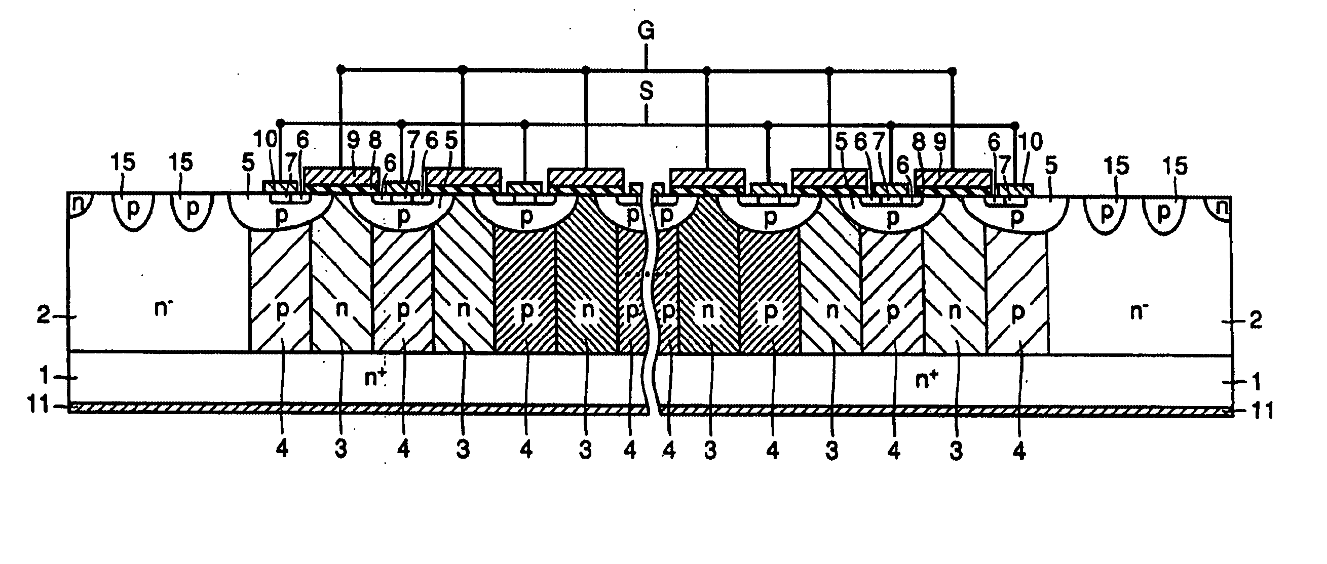
[0244] In the pn-repeating structure in the buried multiple epitaxial layers described so far, a plurality of (for example, three) p-type impurity regions 4 a that form layers in the depth direction of the semiconductor substrate is integrated as shown in FIG. 7 so as to form p-type impurity regions 4 making up the pn-repeating structure. In addition, a plurality of (for example, three) n-type impurity regions 3 a that form layers in the depth direction of the semiconductor substrate is integrated so as to form n-type drift regions 3 making up the pn-repeating structure. Therefore, each of p-type impurity regions 4 and n-type impurity regions 3 has an impurity concentration distribution that periodically changes in the depth direction of the substrate.

[0245] An average impurity concentration of each of the plurality of p-type impurity regions 4 is substantially the same and an average impurity concentration of each of the plurality of n-type drift regions 3 is also substantially th...

ninth to twelfth embodiments

[0252] Next, the structure wherein the present invention is applied to a diode instead of a MOS-FET is described in the ninth to twelfth embodiments.

[0253] The configurations wherein the MOS-FETs in FIGS. 1, 6 and 9 are replaced with diodes are shown in FIGS. 10, 11 and 12 as the ninth, tenth and eleventh embodiments, respectively.

[0254] In reference to FIGS. 10 to 12, a p-type impurity region 21 is formed on the first main surface side of the entirety of the pn-repeating structure so as to be electrically connected to an anode electrode 22.

[0255] Here, the other parts of the configuration of FIG. 10 are approximately the same as in the configuration shown in FIG. 1, the other parts of the configuration of FIG. 11 are approximately the same as in the configuration shown in FIG. 6 and the other parts of the configuration of FIG. 12 are approximately the same as in the configuration shown in FIG. 9 and, therefore, the same symbols are attached to the same members, of which the desc...

thirteenth to sixteenth embodiments

[0261] Next, the structure that is a diode structure, as the above, and wherein the present invention is applied to a diode of which the upper portion has a Schottky junction is described in the thirteenth to sixteenth embodiments.

[0262] The configurations wherein the diodes in FIGS. 10, 11, 12 and 13 are replaced with Schottky diodes are shown in FIGS. 14, 15, 16 and 17 as the thirteenth, fourteenth, fifteenth and sixteenth embodiments, respectively.

[0263] In reference to FIGS. 14 to 17, an anode electrode 22 made of metal is electrically connected to the first main surface of the semiconductor substrate and a metal silicide layer 21a is formed on this connection portion.

[0264] Here, the other parts of the configuration of FIG. 14 are approximately the same as in the configuration shown in FIG. 10, the other parts of the configuration of FIG. 15 are approximately the same as in the configuration shown in FIG. 11, the other parts of the configuration of FIG. 16 are approximately ...


PUM


Abstract

A semiconductor device of the present invention has a pn-repeating structure that a structure in which a p-type impurity region (4) and an n-type drift region (3) are aligned side by side is repeated twice or more, and a low concentration region which is either p-type impurity region (4) or n-type drift region (3) located at the outermost portion of this pn-repeating structure has the lowest impurity concentration or has the least generally effective charge amount among all the p-type impurity regions (4) and n-type drift regions (3) forming the pn-repeating structure. Thereby, the main withstand voltage of a power semiconductor device to which a three dimensional multi-RESURF principle is applied, wherein the element withstand voltage is specifically in the broad range of 20 to 6000 V, can be improved and the trade-off relationship between the main withstand voltage and the ON resistance can also be improved, so that an inexpensive semiconductor device of which the power loss is small and of which the size of the chip is small can be obtained. In addition, a trench of a dotted line trench (DLT) structure and a manufacturing method corresponding to this can be used, so that a semiconductor device with a good yield can be obtained at low cost.

Description

TECHNICAL FIELD [0001] The present invention relates to a semiconductor device and a manufacturing method for the same, and more particularly to an improvement in performance and an increase in the yield of a power semiconductor device. BACKGROUND ART [0002] An element using a repeating microscopic structure of p-type and n-type layers wherein an electric field relaxation phenomenon called the RESURF (REduced SURface Field) effect is applied in place of the uniform n-type drift layer of a conventional MOS-FET (Metal Oxide Semiconductor-Field Effect Transistor) has been proposed in, for example, U.S. Pat. No. 6,040,600. In this element a low ON resistance is obtained in the ON condition due to the n-type drift layer of which the impurity concentration is higher than the concentration of the uniform n drift layer in the conventional structure by approximately one order while in the OFF condition the entire electric field is relaxed due to a three-dimensional multiple RESURF effect of ...

Claims


Application Information

Patent Timeline
Patent Type & Authority Applications(United States)
IPC IPC(8): H01L21/265H01L21/266H01L21/336H01L29/06H01L29/78
CPCH01L21/26586H01L21/266H01L29/0619H01L29/0634H01L29/0649H01L29/0834H01L29/66712H01L29/7801H01L29/7802H01L29/7824H01L29/0653H01L29/7823H01L29/7811H01L21/18
Inventor MINATO, TADAHARUNITTA, TETSUYA
Owner MITSUBISHI ELECTRIC CORP
Why Eureka
Try Eureka