Method for fabricating thermally enhanced semiconductor device

Active Publication Date: 2005-03-03
PHOENIX PRECISION TECH CORP
View PDF1 Cites 65 Cited by
  • Summary
  • Abstract
  • Description
  • Claims
  • Application Information

AI Technical Summary

Benefits of technology

[0013] In the use of the above fabrication method for semiconductor device, at least one semiconductor chip is attached to a heat sink via a thermally conductive adhesive, so as to effectively dissipate heat produced from the chip. The heat sink is usually made of a metallic material, which can provide a good electromagnetic shielding effect for the semiconductor device. The chip is received in an opening of a metal plate, insulating plate or circuit board mounted on the heat sink, such that the overall thickness of the semiconductor device can be reduced for size miniaturization. Moreover, at least one circuit build-up structure is formed on the metal plate, insulating plate or circuit board. The circuit build-up structure comprises at least one insulating layer, circuit layer and conductive vi

Problems solved by technology

However, the above semiconductor package may cause significant problems during practical operation.
Since there are a plurality of electronic elements and electronic circuits densely disposed on the chip, a huge amount of heat would be generated by these electronic elements and circuits; if the heat cannot be efficiently dissipated, the performance and lifetime of the chip may be damaged by overheat.
Further, the semiconductor package lacks a shielding mechanism and thus is easily subject to external electromagnetic interference and noises.
However, the solder balls for connecting the package to the external PCB must be made with a height larger than a height of wire loops of the bonding wires protruding on the back side of the substrate; this arrangement restricts the routability on the substrate and set a limitation on the size of the solder balls.
Moreover, the bonding wires bonded to the chip are densely arranged and easily subject to short circuit if adjacent bonding wires accidentally come into

Method used


Image

  • Method for fabricating thermally enhanced semiconductor device
  • Method for fabricating thermally enhanced semiconductor device
  • Method for fabricating thermally enhanced semiconductor device

Examples


Embodiment Construction

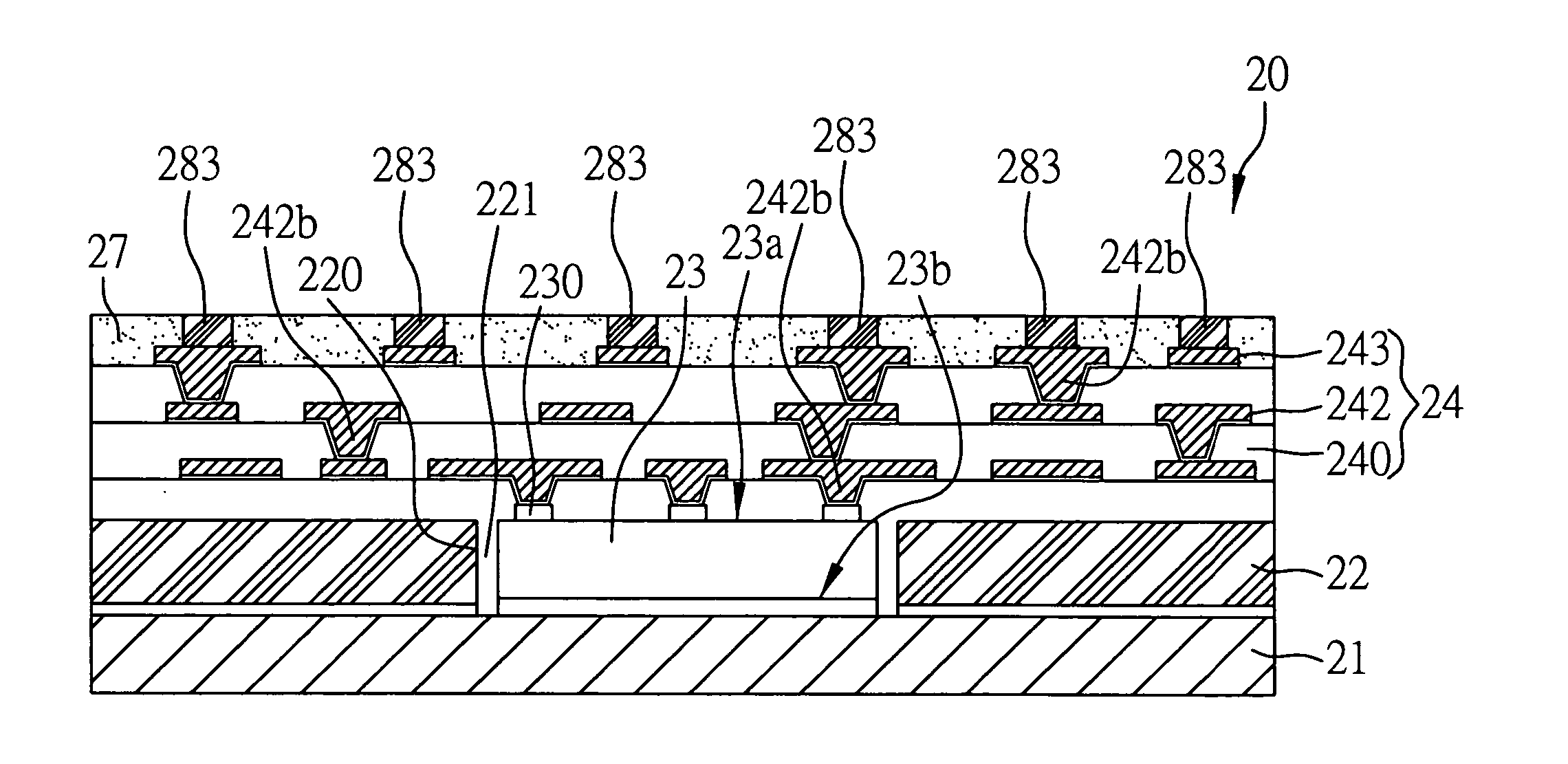
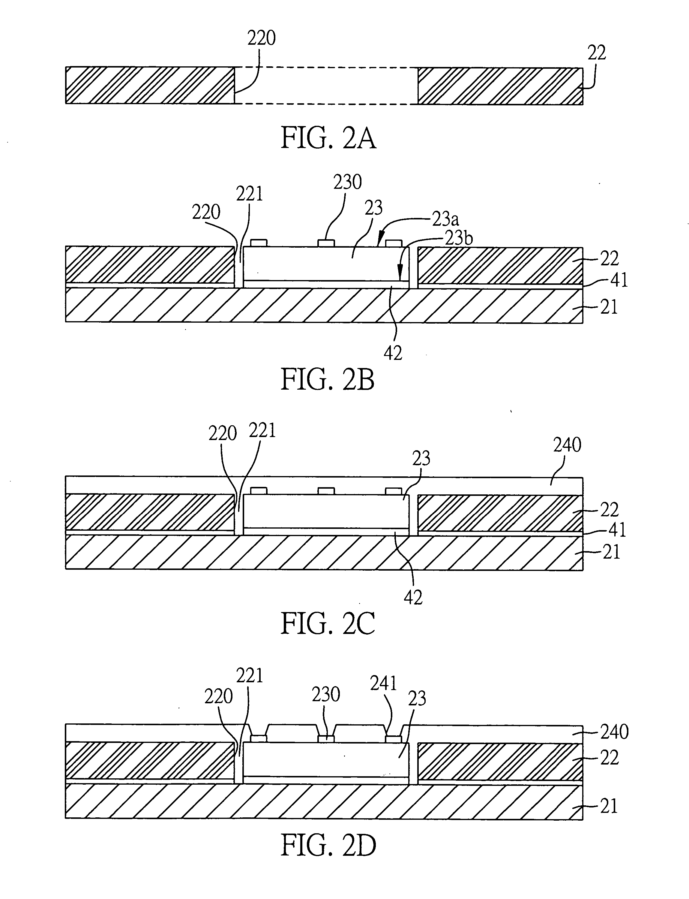
[0019] The preferred embodiments of a thermally enhanced semiconductor device and its fabrication method proposed in the present invention are described with reference to FIGS. 2A-2K and 3.

[0020]FIGS. 2A-2K show a series of procedural steps of the method for fabricating a thermally enhanced semiconductor device according to a first preferred embodiment of the present invention.

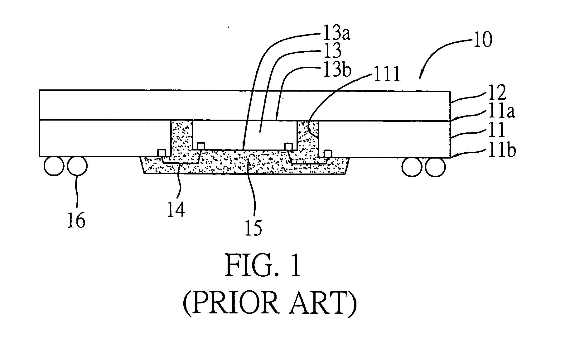
[0021] Referring to FIG. 2A, a support plate 22 is prepared, which can be a metal plate, insulating plate or circuit board. The support plate 22 is formed with at least one opening 220 penetrating through the same. The metal plate can be made of copper. The insulating plate can be made of epoxy resin, polyimide resin, cyanate ester, carbon fiber, BT (bismaleimide triazine) resin, or a mixture of epoxy resin and fiber glass. The circuit board can be a pre-treated multi-layer circuit board, which is composed of a core layer with a conductive metal layer formed on at least one surface of the core layer; next th...


PUM


Abstract

A method for fabricating a thermally enhanced semiconductor device. A support plate having at least one opening is mounted on a heat sink. At least one chip is mounted on the heat sink and received in the opening. An insulating layer is formed over the chip and the support plate and filled in the opening. A plurality of vias are formed in the insulating layer to expose electrode pads on the chip. A conductive layer is deposited on the insulating layer and the exposed electrode pads. A resist layer is formed on the conductive layer and patterned to expose a predetermine part on the conductive layer. Then, a patterned circuit layer is deposited on the exposed part of the conductive layer by electroplating. The patterned resist layer and the conductive layer underneath the patterned resist layer are removed. A plurality of conductive elements are formed on the circuit layer.

Description

FIELD OF THE INVENTION [0001] The present invention relates to methods for fabricating thermally enhanced semiconductor devices, and more particularly, to a method for fabricating a semiconductor device incorporated with a heat sink, at least one chip and at least one circuit build-up structure. BACKGROUND OF THE INVENTION [0002] The evolution of the packaging technology has developed various types of semiconductor packages. For example, BGA (ball grid array) package employs advanced packaging technology to mount a semiconductor chip on a front side of a substrate and use the self-alignment technique to form an array of solder balls on a back side of the substrate. This allows a unit area on the substrate or chip carrier to accommodate more solder balls or input / output (I / O) connections to be suitable for the chip that is highly integrated, and the solder balls or I / O connections are used to bond and electrically connect the semiconductor package to an external device such as printe...

Claims


Application Information

Patent Timeline
IPC IPC(8): H01L21/4763H01L21/60H01L23/34H01L23/36H01L23/498
CPCH01L23/36H01L2924/01033H01L24/19H01L24/24H01L2221/68345H01L2224/04105H01L2224/20H01L2224/24227H01L2224/48095H01L2924/01029H01L2924/01078H01L2924/01082H01L2924/15153H01L2924/1517H01L2924/15311H01L2924/15312H01L2924/1532H01L2924/3025H01L23/49816H01L2924/01024H01L2924/01006H01L24/48H01L2924/00014H01L2924/12042H01L2924/181H01L2224/32245H01L2224/73267H01L2924/00H01L2924/00012H01L2224/45099H01L2224/45015H01L2924/207
Inventor HSU, SHIH-PING
Owner PHOENIX PRECISION TECH CORP
Why Eureka
Try Eureka