
In situ determination of resistivity, mobility and dopant concentration profiles

Active Publication Date: 2005-03-10
ACTIVE LAYER PARAMETERICS
View PDF6 Cites 30 Cited by
  • Summary
  • Abstract
  • Description
  • Claims
  • Application Information

AI Technical Summary

Benefits of technology

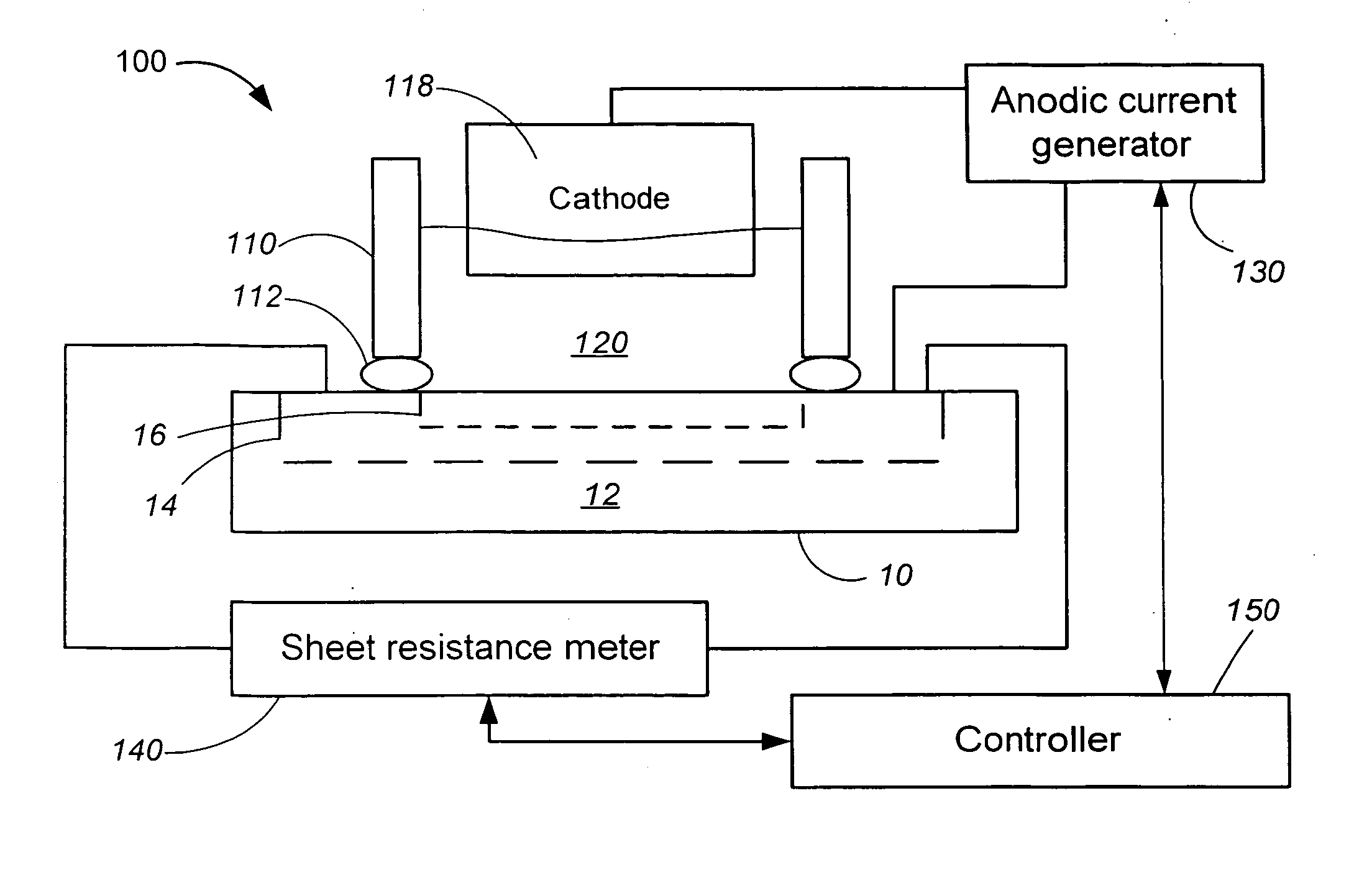
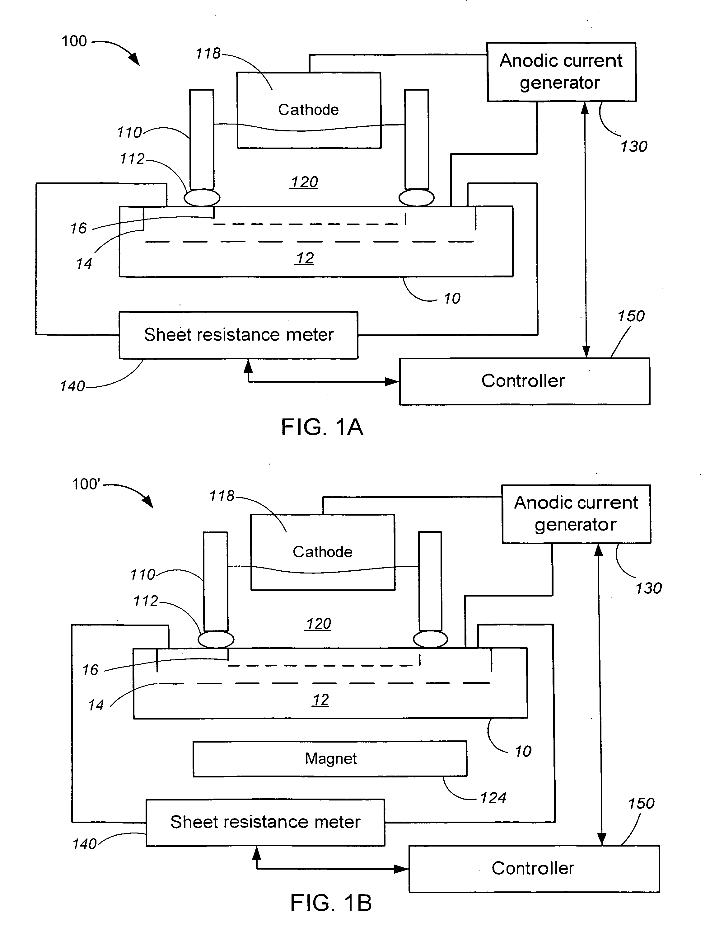
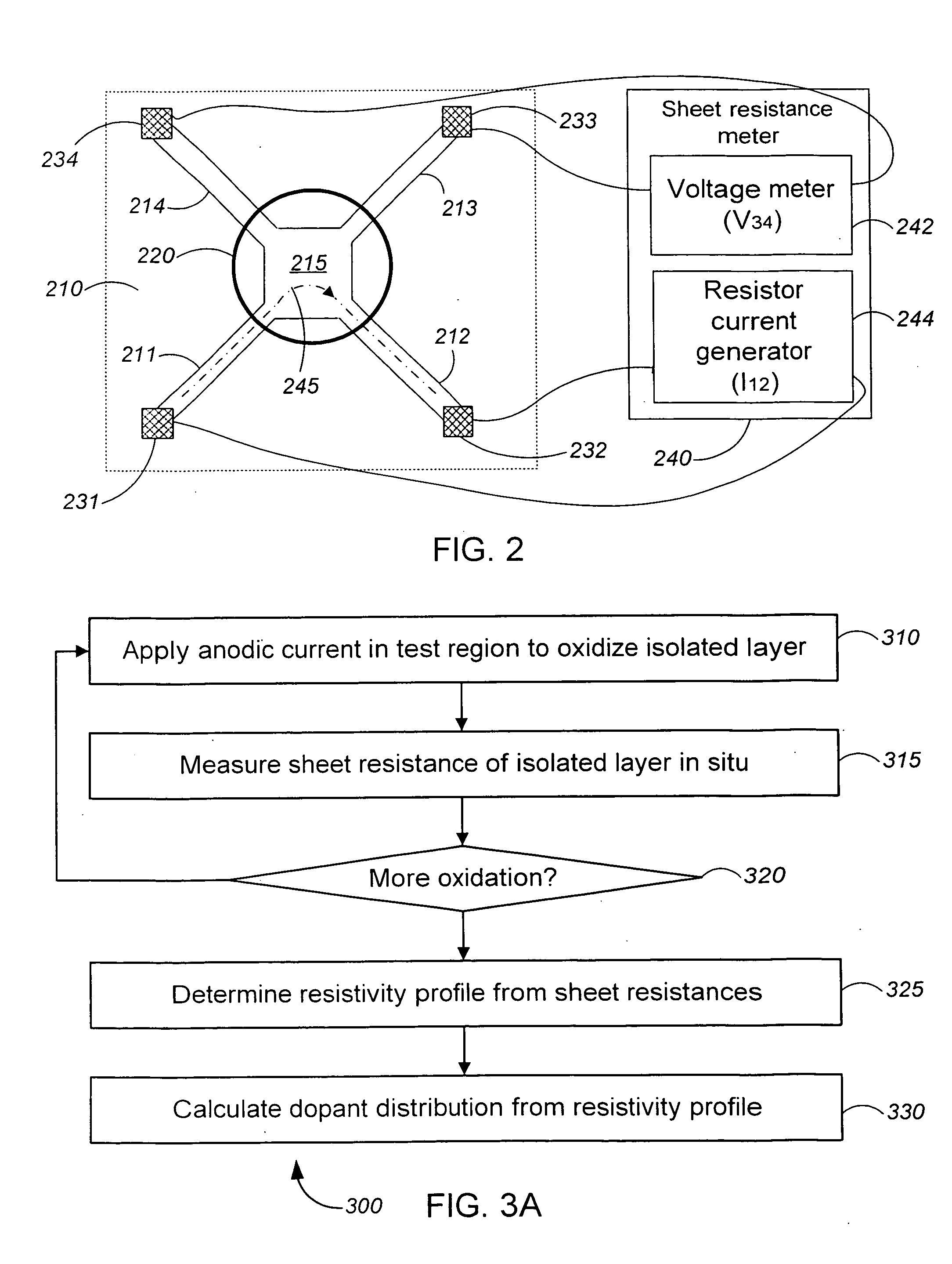
The invention can make use of one or more of the following phenomena: 1. The thickness of anodic oxide formed is proportional to the forming voltage developed so that measurement of forming voltage permits accurate determination of the oxide thickness. 2. The growth of an anodic oxide film effectively removes a calculable thickness of doped silicon from the resistor circuit. 3. The thickness of silicon consumed is linearly related to the thickness of oxide formed. 4. The anodic oxide formed acts as an insulator, electrically isolating the silicon resistor from the electrolyte. 5. The use of a van der Pauw resistor permits the calculation of the sheet resistance to be independent of the resistor dimensions. 6. The use of the cross design of a van der Pauw resistor permits the sheet resistance measurement to be made over a very small area, the area at the junction of the four resistor arms. 7. The use of a liquid-containing electrode fixture permits us to anodically oxidize a doped silicon surface over a very small area. 8. The use of permanent magnets permits the introduction of high magnetic fields from the underside of the test specimen.
Equipment which incorporates these features permits us to effectively carry out a series of sheet resistance measurements (e.g., conventional sheet resistance or Hall sheet resistance) on a doped silicon surface from which thin incremental layers are sequentially removed. The incremental increase in sheet resistance (conventional and Hall sheet coefficient) enables the calculation, in a direct and simple manner, of the resistivity profile, the mobility profile, and the concentration distribution. A simplified technique which omits the measurement carried out under a magnetic field enables the calculation of the resistivity profile, which is often the only information desired.
This invention is particularly adapted for directly measuring the resistivity and dopant concentration profiles of ultra-shallow junctions down to atomic dimensions. The sheet resistances measured with anodic oxide growth corresponding to a forming voltage increment of 2 Volts are measured at silicon depth increments of 4.4 angstroms (for comparison the width of an atomic layer of silicon is 2.71 angstroms). The measurements described by the invention require only a small area of the silicon surface and can be carried out on the test area of a large production wafer without damaging the wafer. Thus this permits this invention to be used for process monitoring in the production process.

Problems solved by technology

However, this differential Hall effect (DHE) technique was subject to the time and labor limitations of the Tannebaum anodic oxidation stripping technique.
This technology requires a high cost equipment and highly trained operators.

Method used


Image

  • In situ determination of resistivity, mobility and dopant concentration profiles
  • In situ determination of resistivity, mobility and dopant concentration profiles
  • In situ determination of resistivity, mobility and dopant concentration profiles

Examples


experimental implementation

Sample Preparation

The test structures used to evaluate this technique were prepared on the surfaces of wafers which had been subjected to blanket implantations. N-type wafers with a donor concentration of 2×1014 cm−3 were implanted with a dose of 1×10¹⁵ BF2 cm−2 at an energy of 5 keV. P-type wafers with an acceptor concentration of 1×1015 cm−3 were implanted with a dose of 1×10¹⁵ As cm−2 at an energy of 2 keV. These wafers were subjected to a rapid thermal anneal of 10 seconds at 1000 degrees Celsius.

The test structures were prepared by applying photoresist to the surfaces, and applying UV light through a mask, which delineated the test pattern. After the development of this pattern, the use of XeF2 gas etching, a standard production technique, produced test structures similar to that as shown in FIG. 2 with a cross-section as shown in FIG. 6C.

Apparatus

Four items of equipment were used. The first was a mount for the specimen. The van der Pauw resistor was prepared on a sili...


PUM


Abstract

The present invention provides techniques for an in-situ measurement of resistivity profiles and dopant concentration distributions in semiconductor structures, such as shallow junctions. A substrate with a resistor test structure having a conduction circuit may be placed at a measurement station, surface layers may be successively removed from the conduction circuit at the measurement station, a sheet resistance of the conduction circuit may be measured at the measurement station after the removal of each surface layer to generate a plurality of sheet resistance measurements, and the resistivity profile may be calculated from the plurality of sheet resistance measurements.

Description

BACKGROUND This invention relates to characterizing semiconductor structures. Shortly after the commercial development of the transistor and other structures built on semiconductor substrates, a four-point probe was introduced to measure the sheet resistance of doped semiconductor layers. (See for example, L. B. Valdes, Proc. IRE, Volume 42, 1954, or in A.S.T.M. Standard F374, Annual Book of A.S.T.M. Standards Vol. 10.05.) To measure dopant concentration as a function of depth in a substrate, layers were successively removed from the substrate by abrasive lapping or chemical etching. After removing each layer at a processing station, the substrate was transferred to a measurement station to measure the sheet resistance. As layers of known thickness are removed, the sheet resistance changes. From these changes, a resistivity profile can be calculated, and converted into a dopant concentration distribution based on an assumption of mobility values which provide a relationship betwee...

Claims


Application Information

Patent Timeline
IPC IPC(8): G01N27/04G01R31/26G01R31/28H01L23/544
CPCG01N27/041G01R31/2648G01R31/2831H01L22/14H01L22/34H01L2924/0002H01L2924/014H01L2924/00
Inventor PRUSSIN, SIMON A.
Owner ACTIVE LAYER PARAMETERICS
Learn More