
Method for isotropic etching of copper

Inactive Publication Date: 2005-03-17
IBM CORP
View PDF7 Cites 36 Cited by
  • Summary
  • Abstract
  • Description
  • Claims
  • Application Information

AI Technical Summary

Benefits of technology

[0077] The foregoing description of the invention illustrates and describes the present invention. Additionally, the disclosure shows and describes only the preferred embodiments of the invention but, as mentioned above, it is to be understood that the invention is capable of use in various other combinations, modifications, and environments and is capable of changes or modifications within the scope of the inventive concepts as expressed herein, commensurate with the above teachings and / or the skill or knowledge of the relevant art. The embodiments described hereinabove are further intended to explain best modes known of practicing the invention and to enable others skilled in the art to utilize the invention in such, or other, embodiments and with various modifications required by the particular applications or uses of the invention. Accordingly, the description is not intended to limit the invention to the form disclosed herein also, it is intended that the appended claims be construed to include alternative embodiments. All publications and patent applications cited in this specification are herein incorporated by reference as if each individual publication or patent application were specifically and individually indicated to be incorporated by reference.

Problems solved by technology

Any roughening of this surface can cause significant process or electrical variability to the structures.
Although commercial cleaning solutions exist for this, these are usually extremely costly.

Method used


Image

  • Method for isotropic etching of copper
  • Method for isotropic etching of copper
  • Method for isotropic etching of copper

Examples


example 1

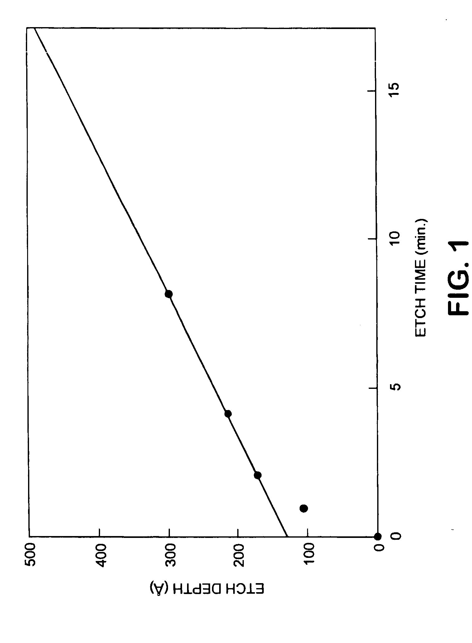
[0068] An interconnect copper structure, which includes a dielectric and a liner inert to the etchant and containing 1 and 0.1 micron wide wires, was first cleaned with a deaerated isopropanol / HCl mixture (25% IPA, 0.18% HCl) to remove any contaminants from the preceding CMP (chemical-mechanical polishing) step, and then was etched for about 4 minutes at room temperature in an etchant of this invention (an aqueous solution containing 2.94 wt % H2O2, 0.54% NH3, and 0.05% CDTA and a pH of approximately 10.2). During the etching the sample was stationary in a beaker and the solution was stirred with a 2.5 cm magnetic stirring bar at 180 rpm. The sample was then dried in a nitrogen stream. The inhibiting layer was then removed by treating the sample for about 4 minute with a nitrogen-deaerated 100:1 (v / v) acetic acid solution.

[0069] This example illustrates the steps of inhibiting layer formation and dissolution with respect to effects on copper recessing. See FIGS. 4, 5 and 6 which sh...

example 2

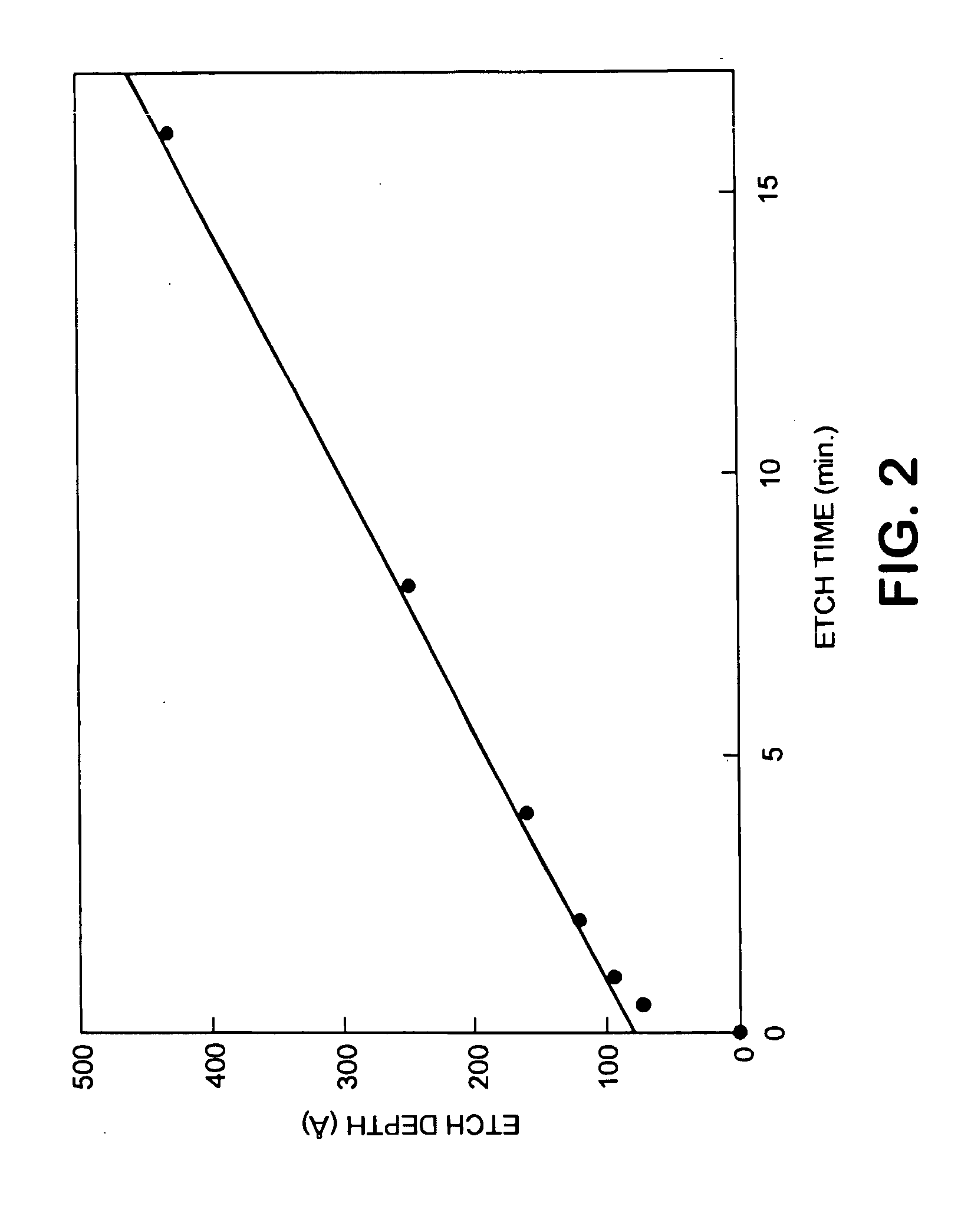
[0073] A substrate similar in type to the one used in Example 1, was cleaned as described above and then was etched for 8 minutes in the same etching solution as used in Example 1 and under the same conditions as above. The inhibiting layer was immediately removed by treating the sample for about 2 minutes with a nitrogen-deaerated mixture of 0.2 Molar sulfuric acid and 0.2 Molar acetic acid.

[0074] This example demonstrates the possibility of deeper recesses which in turn shows that the etch according to the present invention is not self limiting as is the known art. This example also demonstrates that the present invention make possible smoother copper recesses than typical etchants as, for instance, exemplified in example 3 below.

[0075] The results are shown in FIG. 7. FIG. 7 is an AFM image of a 3×5 micron copper pad imbedded in a dielectric after processing with CMP and IPA / HCl clean, followed by an 8 minute etch according to the present invention and the as acid removal of th...

example 3

[0076] A sample similar in type to the one used in example 2 was etched in a standard Cu etch (H2O:H2O2 30%: acetic acid 1000:3:5 v / v). The average depth of the copper below the dielectric surface is about 54 nanometers. Note the roughness that occurs due to the non-uniform copper removal (AFM surface topograph, FIG. 8) as compared to the smooth copper surface achieved by the present invention (see FIGS. 6 and 7).


PUM

PropertyMeasurementUnit
Thicknessaaaaaaaaaa
Molar densityaaaaaaaaaa

Abstract

Copper and copper alloys are etched to provide uniform and smooth surface by employing an aqueous composition that comprises an oxidant, a mixture of at least one weak complexant and at least one strong complexant for the copper or copper alloy, and water and has a pH of about 6 to about 12 so as to form an oxidized etch controlling layer and to uniformly remove the copper or copper alloy; and then removing the oxidized etch controlling layer with a non-oxidizing composition. Copper and copper alloy structure, having smooth upper surfaces are also provided.

Description

TECHNICAL FIELD [0001] The present invention relates to a process for etching copper and copper alloys, and particularly isotropic etching to provide uniform and smooth copper surfaces. The present invention is also concerned with copper or alloy structures exhibiting uniform and smooth copper surfaces. BACKGROUND OF THE INVENTION [0002] In the fabrication of thin film wiring for electronic applications, it is often required to etch polycrystalline copper surfaces. Any roughening of this surface can cause significant process or electrical variability to the structures. Current etchants show significant surface roughening, as well as dependence of etching rates on feature density, size, electrical connectivity, and location on the wafer. In particular, commonly used copper etchants, such as acid solutions of peroxide or persulfate, tend to preferentially etch the copper in the immediate proximity of grain boundaries. In addition, different exposed crystal faces tend to etch at differ...

Claims


Application Information

Patent Timeline
IPC IPC(8): C23C22/63C23F1/34C23G1/10H01L21/3213
CPCC23C22/63H01L21/32134C23G1/103C23F1/34
Inventor COOPER, EMANUEL I.FURMAN, BRUCE K.RATH, DAVID L.
Owner IBM CORP
Features
  • Generate Ideas
  • Intellectual Property
  • Life Sciences
  • Materials
  • Tech Scout
  • Unparalleled Data Quality
  • Higher Quality Content
  • 60% Fewer Hallucinations
Learn More