Fully-depleted castellated gate MOSFET device and method of manufacture thereof

a castellated gate and mosfet technology, applied in the field of field effect transistors, can solve the problems of reducing the power consumption of digital functions, and reducing the number of significant problems

Active Publication Date: 2005-03-17
IP3 2021 SERIES 600 OF ALLIED SECURITY TRUST I
View PDF2 Cites 218 Cited by
  • Summary
  • Abstract
  • Description
  • Claims
  • Application Information

AI Technical Summary

Benefits of technology

Accordingly, it is one object of the present invention to provide an impr

Problems solved by technology

While CMOS scaling has enabled the circuit and system designer to pack a tremendous amount of functionality onto a silicon die, it has simultaneously created a number of significant problems as far as the chip's ability to interface with the outside world.
Unfortunately, in such technology evolution, the thick oxide I/O device has become somewhat of a “forgotten stepchild”, as only the thin-oxide core devices can truly take advantage of the shrinking feature sizes that are enabled by state-of-the-art photolithography.
More importantly, as the thick oxide device is a “leftover” from the previous technology node, it typically under-performs the thin-oxide core device in terms of speed/bandwidth (ft).
While this reliability-driven voltage trend results in lower power consumption for digital functions, the effect is not necessarily the same in the analog case.
In fact, it has been shown that in an analog-to-digital converter application with a fixed dynamic range requirement, power consumption can actually increase with decreasing power supply.
More problematic from the standpoint of device reliability and survivability is the significantly harsher EMI (electromagnetic induction)/ESD (electrostatic discharge) environment seen by I/O devices used in mixed-signal communications applications.
However, in a data transmission or communication situation, there is the additional problem of signal reflections due to improperly terminated transmission lines.
In the first two mixed-signal examples, that is system backplane and chip-to-chip, a termination problem could chronically arise due to manufacturing tolerances, or as the res

Method used


Image

  • Fully-depleted castellated gate MOSFET device and method of manufacture thereof
  • Fully-depleted castellated gate MOSFET device and method of manufacture thereof
  • Fully-depleted castellated gate MOSFET device and method of manufacture thereof

Examples


embodiment 72

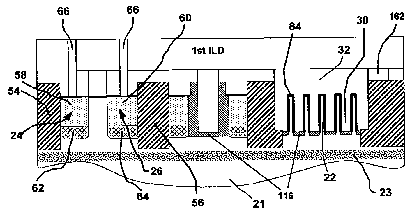
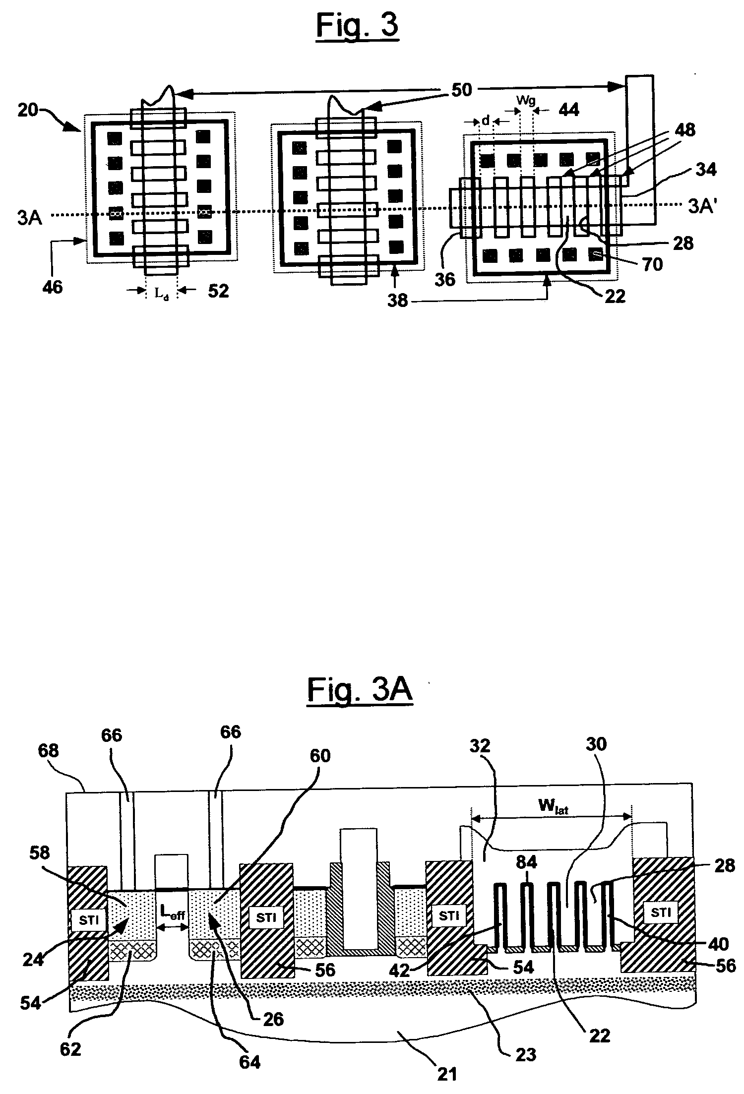
The contacts 66 to the source and drain structures 24, 26 may be coincident with the upper silicon surface, or contacts 67 (as shown in FIG. 4A) may penetrate into the uppermost impurity layer depending on the desired device electrical characteristics. For example, surface contacts 66 could result in higher series resistance, which would be beneficial in enhancing ESD characteristics. In the particular example of FIGS. 3 and 3A, the contact masks 70 are laid-out in such a way as to be directly in-line with the conductive channels 22. This approach should provide the least device series resistance, thus improving device performance. Furthermore, it should be understood that additional process steps can be added to the overall fabrication sequence to shut-down the bottom gate. Examples are illustrated in the case of a dual-gate embodiment 72 illustrated in FIGS. 4 and 4A, including the addition of a highly doped “global” buried layer 74, preferably p-type for an NMOS device, and botto...

embodiment 78

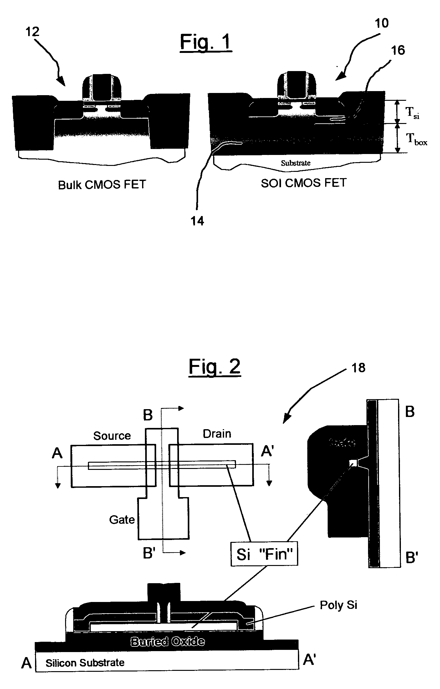
FIGS. 5 and 5A illustrate an NMOS device embodiment 78 of the disclosed device invention using a silicon-on-insulator (SOI) starting substrate 80. Note that the device mask layout remains substantially the same as the case of the device 20 with the bulk starting wafer 21 shown in FIGS. 3-3A. Substantially similar to the bulk silicon substrate device 20, the device 78 includes a plurality of thin silicon channel elements 22 that span the distance between a source region 24 and a drain region 26. In the SOI wafer case of the device 78, the device's gate slots 82 can be etched to the same depth as the STI islands 54, 56, that is all the way to the buried oxide 75. However, there are advantages to leaving a common silicon connection in the form of the substrate 21 of FIGS. 3 and 3A at the bottom, thus enabling the use of body contacts which can be employed to eliminate device snapback problems as well as provide a path of higher thermal conductivity with which to dissipate heat.

In the ...

second embodiment

In this second method embodiment, penetration of the source and drain implant 24, 26 into the polysilicon 150 is no longer a concern. However, the nitride cap layer 154 provides 50% higher stopping power than polysilicon, thus extending the depth to which the source and drains 24, 26, and therefore the channel slots 22, can be fabricated. The purpose of the polysilicon 150 as the bottom stack layer is so that any spacers or stringers that are formed can be removed utilizing an ashing step. Thus, an advantage of this second embodiment is that the entire dummy gate stack 149 is used to self-align the source and drain implants 24, 26, which provides the opportunity to increase the device drive current with higher aspect ratio gate trenches.

The thickness of the total gate stack 149 must provide the net stopping power to block the implant that forms the bottom portions 62, 64 of the lower source and drain structure 24, 26 (p-type in the case of an NMOS device) from penetrating into the ...


PUM


Abstract

A fully depleted castellated-gate MOSFET device is disclosed along with a method of making the same. The device has robust I/O applications, and includes a semiconductor substrate body having an upper portion with an upper end surface and a lower portion with a lower end surface. A source region, a drain region, and a channel-forming region between the source and drain regions are all formed in the semiconductor substrate body. trench isolation insulator islands surround the source and drain regions as well as the channel-forming region. The channel-forming region is made up of a plurality of thin, spaced, vertically-orientated conductive channel elements that span longitudinally along the device between the source and drain regions. A gate structure is also provided in the form of a plurality of spaced, castellated gate elements interposed between the channel elements. The gate structure also includes a top gate member which interconnects the gate elements at their upper vertical ends to cover the channel elements. Finally, a dielectric layer is provided to separate the conductive channel elements from the gate structure.

Description

BACKGROUND OF THE INVENTION 1. Field of the Invention The present invention relates generally to field effect transistors (FET's) formed as complimentary metal oxide semiconductor (CMOS) structures and, more particularly, to new and improved MOSFET devices having vertically oriented channel structures capable of fully depleted operation at short channel lengths, thereby providing a device for robust I / O applications. Specifically, the present invention relates to an improved MOSFET device and method of fabrication that provides high performance analog and mixed-signal solutions useful in a wide variety of applications. 2. Description of the Prior Art The progression of CMOS device scaling, that is planer MOSFET, has seen a continuous shrinking of transistor dimensions in both the vertical and the horizontal dimensions resulting in an approximate doubling of the number of transistors per unit area every 18 months or so. From the economics perspective, this scaling progression has...

Claims


Application Information

Patent Timeline
IPC IPC(8): H01L21/336H01L21/84H01L27/12H01L29/423H01L29/786
CPCH01L21/84H01L27/1203H01L29/42384H01L29/78636H01L29/66795H01L29/785H01L29/78612H01L29/66545
Inventor SELISKAR, JOHN J.
Owner IP3 2021 SERIES 600 OF ALLIED SECURITY TRUST I
Why Eureka
Try Eureka