
CMOS imaging system with low fixed pattern noise

a technology of fixed pattern noise and imaging system, which is applied in the field of cmos imaging devices, can solve the problems of limited sensor performance and the lowest power dissipation possible for specific video rate, and achieve the effect of high efficiency

Active Publication Date: 2005-03-31
SAMSUNG ELECTRONICS CO LTD
View PDF31 Cites 25 Cited by
  • Summary
  • Abstract
  • Description
  • Claims
  • Application Information

AI Technical Summary

Benefits of technology

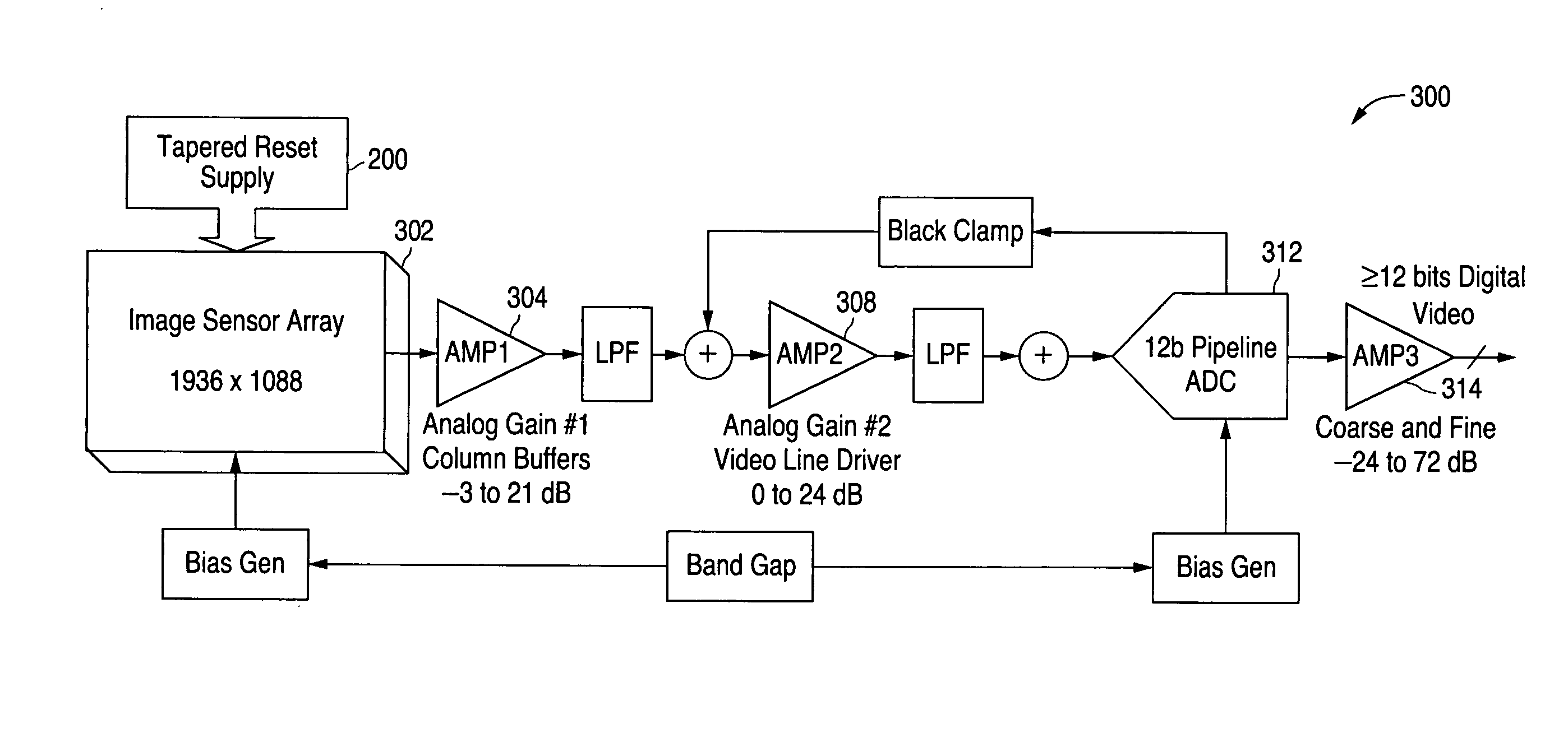
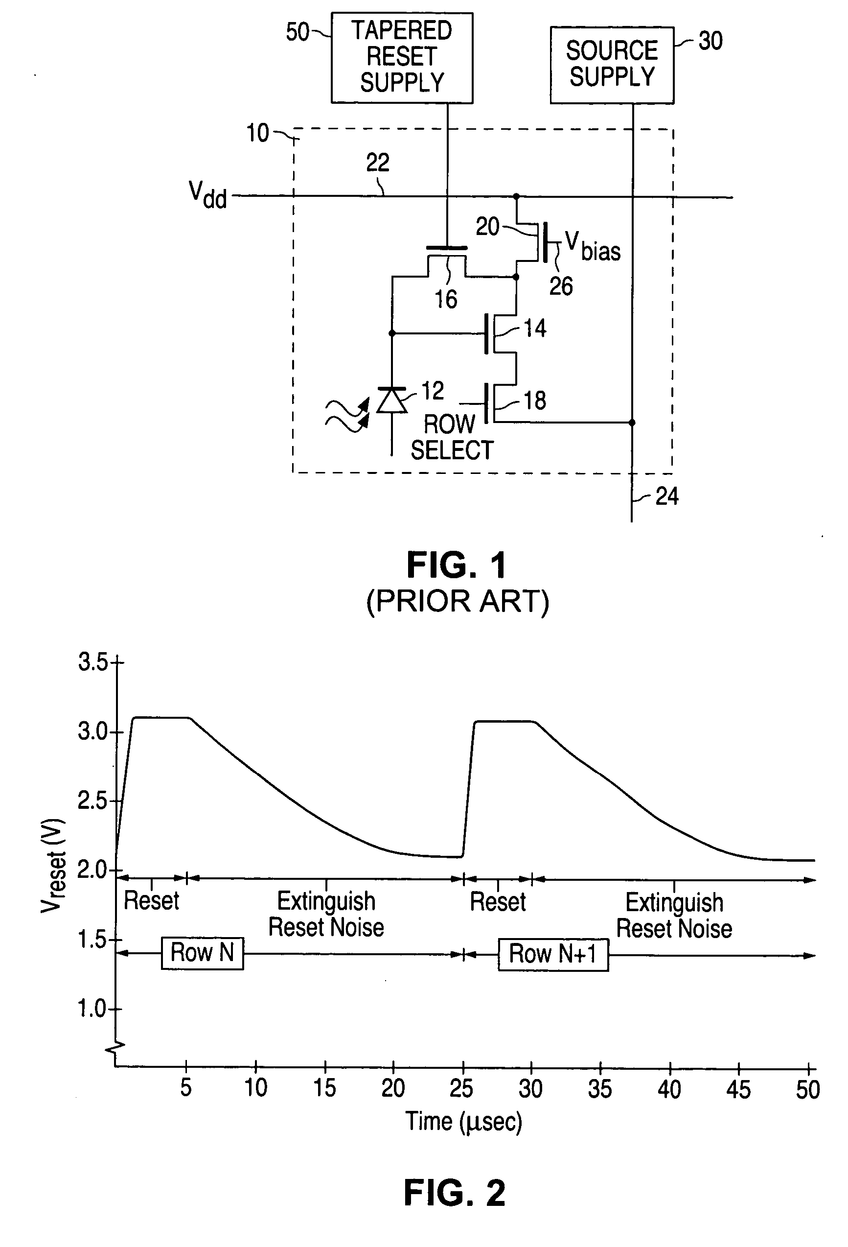
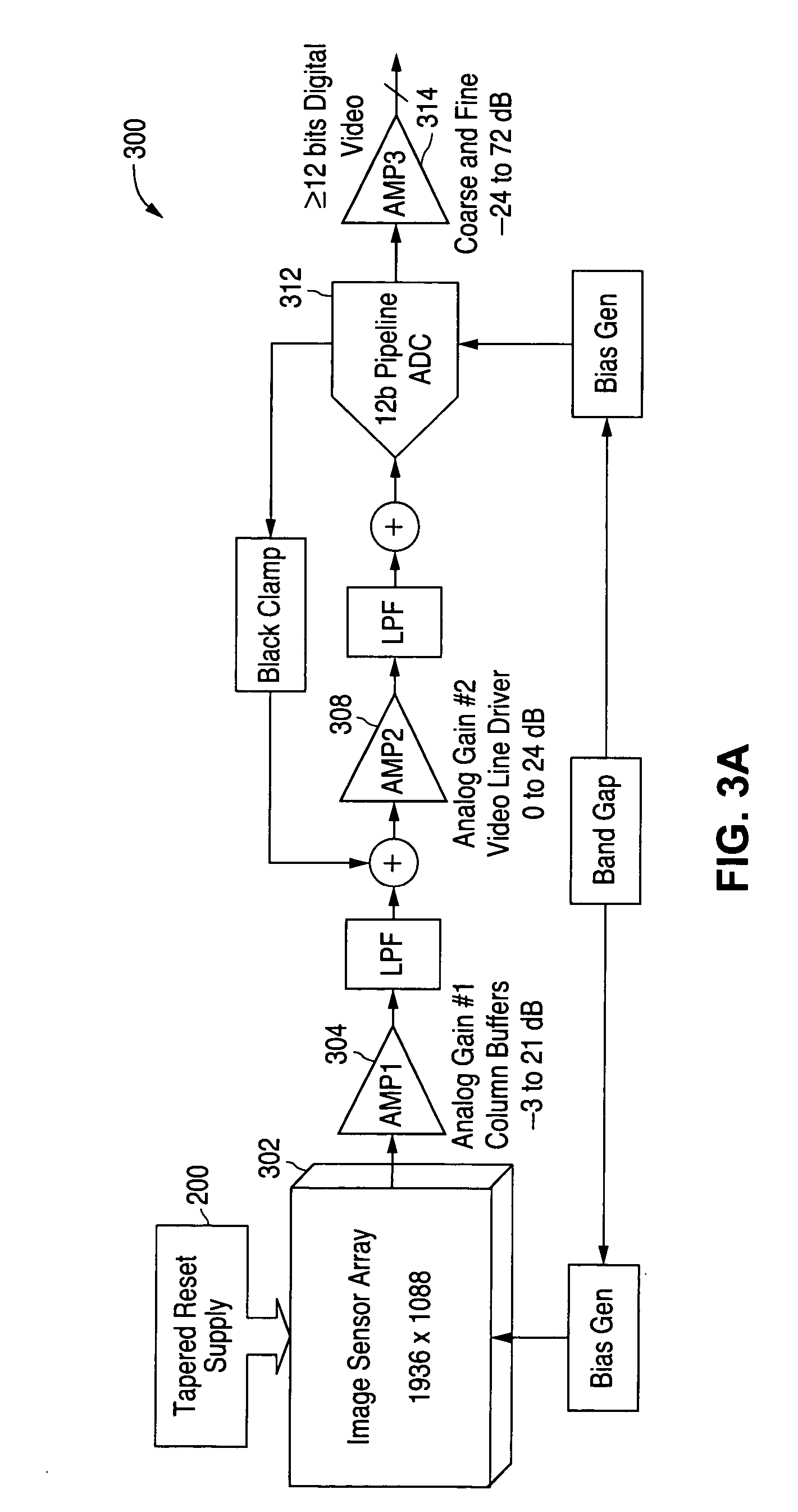
Specifically, in one embodiment, the present circuit comprises three transistors having the same polarity, and a photodetector for each pixel. The present circuit is compact and compatible with pixel pitch below 3 μm using 0.18 μm CMOS fabrication technology. Being a distributed inverter amplifier wherein amplifier components are located both within the pixel and outside of the pixel, the present circuit is compact and compatible with pixel pitch below 3 μm using 0.18 μm CMOS fabrication technology. An access supply connected to the active pixel circuit is a current source that acts as a distributed feedback amplifier, when it is connected to the pixel transistors. The access supply connects to an access MOSFET that isolates a common node from an output node. The system further includes a column buffer, having programmable gain and automatic fixed-pattern noise (FPN) suppression, a video buffer having programmable gain and bandwidth, and a highly efficient A / D converter co-located with the sensor, such that the effective transmission path between the final video buffer and the A / D converter acts primarily as a resistance, rather than a reactance.

Problems solved by technology

By subsequently digitizing the multiplexed signal from the column buffers with one or relatively few high-speed A / D converters in close proximity to the final video buffer, the sensor's performance is still limited only by the temporal noise floor of the CMOS pixel and the chip power dissipation is the lowest possible for the specific video rate.

Method used


Image

  • CMOS imaging system with low fixed pattern noise
  • CMOS imaging system with low fixed pattern noise
  • CMOS imaging system with low fixed pattern noise

Examples


Embodiment Construction

The following description is provided to enable any person skilled in the art to make and use the invention and sets forth the best modes contemplated by the inventor for carrying out the invention. Various modifications, however, will remain readily apparent to those skilled in the art, since the basic principles of the present invention have been defined herein specifically to provide a low noise imaging system with low fixed-pattern noise. Any and all such modifications, equivalents and alternatives are intended to fall within the spirit and scope of the present invention.

The present invention has the advantages of full process compatibility with standard salicided (self-aligned silicide) submicron CMOS. This helps maximize yield and minimize die cost because the circuit complexity is distributed amongst the active-pixels and peripheral circuits, and exploits signal-processing capability inherent to CMOS. The invention's spectral response encompasses the near-ultraviolet (400 ...


PUM


Abstract

A CMOS imager system comprising an active pixel sensor having an access supply which provides distributed feedback, a column buffer (having gain and FPN suppression), and an A / D converter co-located with the sensor such that the effective transmission path between the column buffer (or optional analog PGA) and the A / D converter acts as a resistor, rather than a reactance. The system may further include both an analog gain amplifier stage and a digital programmable amplifier stage.

Description

BACKGROUND OF THE INVENTION This application claims the benefit of U.S. Provisional Application No. 60 / 507,346, filed Sep. 30, 2003, entitled CMOS IMAGING SYSTEM WITH LOW FIXED PATTERN NOISE, the disclosure of which is herein incorporated by reference. 1. Field of the Invention The present invention relates generally to CMOS imaging devices, and more particularly to an imaging system-on-chip implementation for producing high performance image sensors having high resolution, low power dissipation and noise. 2. Description of the Related Art Visible imaging systems implemented in CMOS significantly reduce video camera cost and power by efficiently combining the image sensor with the ancillary components including drive electronics and output signal conditioning electronics. A video camera, for example, can be configured as a single CMOS integrated circuit supported by only an oscillator and a battery. Such a CMOS imaging system-on-chip requires lower voltages and dissipates less ...

Claims


Application Information

Patent Timeline
Patent Type & Authority Applications(United States)
IPC IPC(8): H01LH04N3/14H04N25/00
CPCH03F3/005H03F3/082H04N5/378H04N5/365H04N5/3745H04N5/363H04N25/65H04N25/77H04N25/78H04N25/677H04N25/76H04N25/67H04N25/75
Inventor KOZLOWSKI, LESTER J.LOOSE, MARKUS
Owner SAMSUNG ELECTRONICS CO LTD
Learn More