

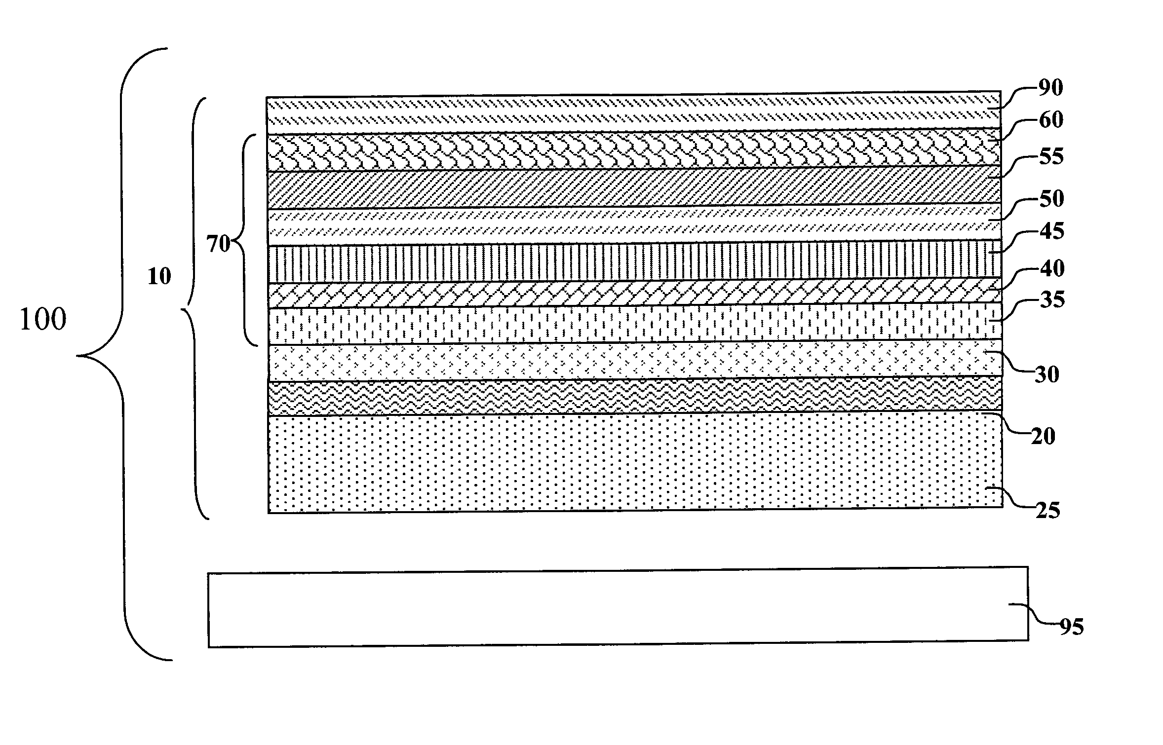
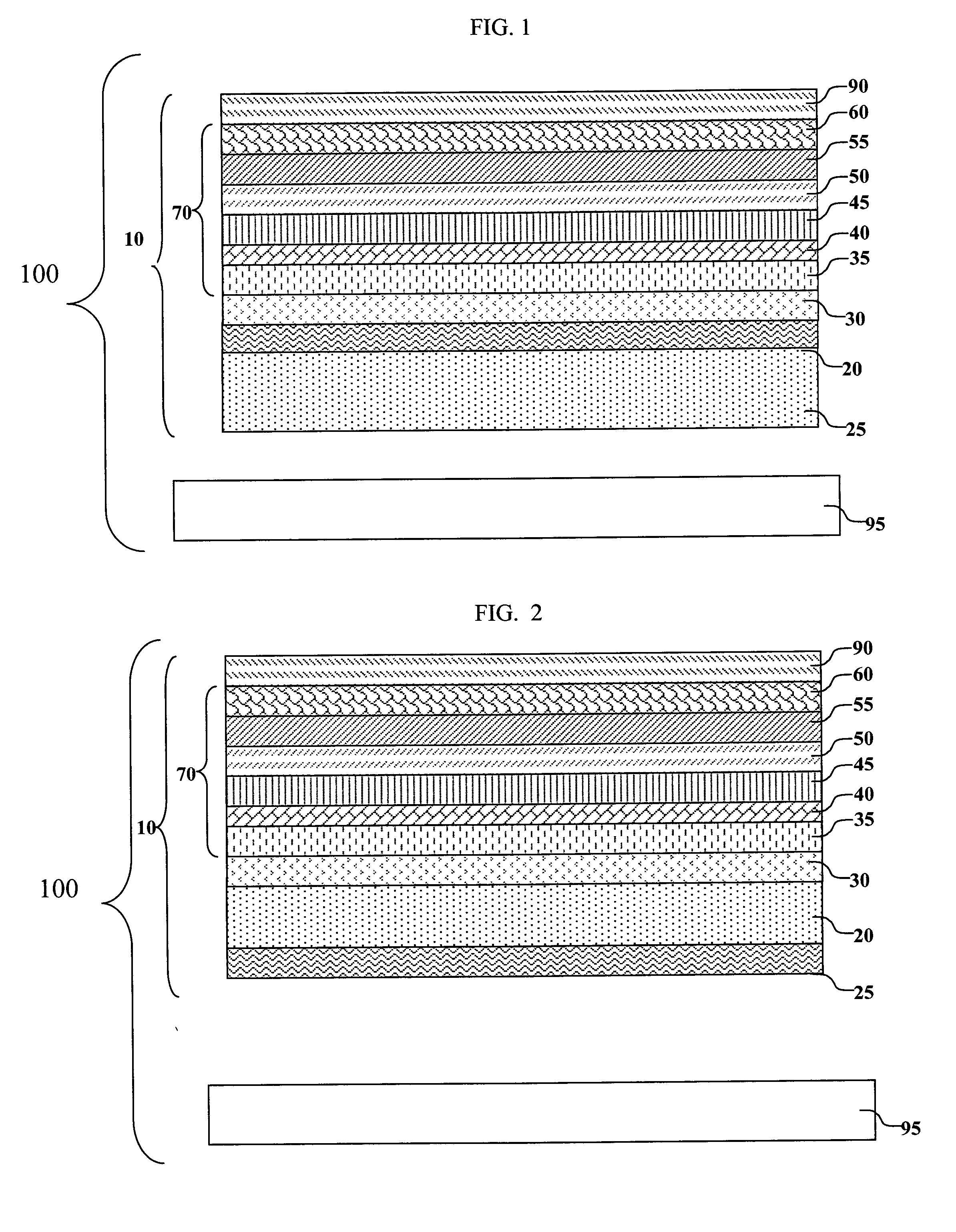
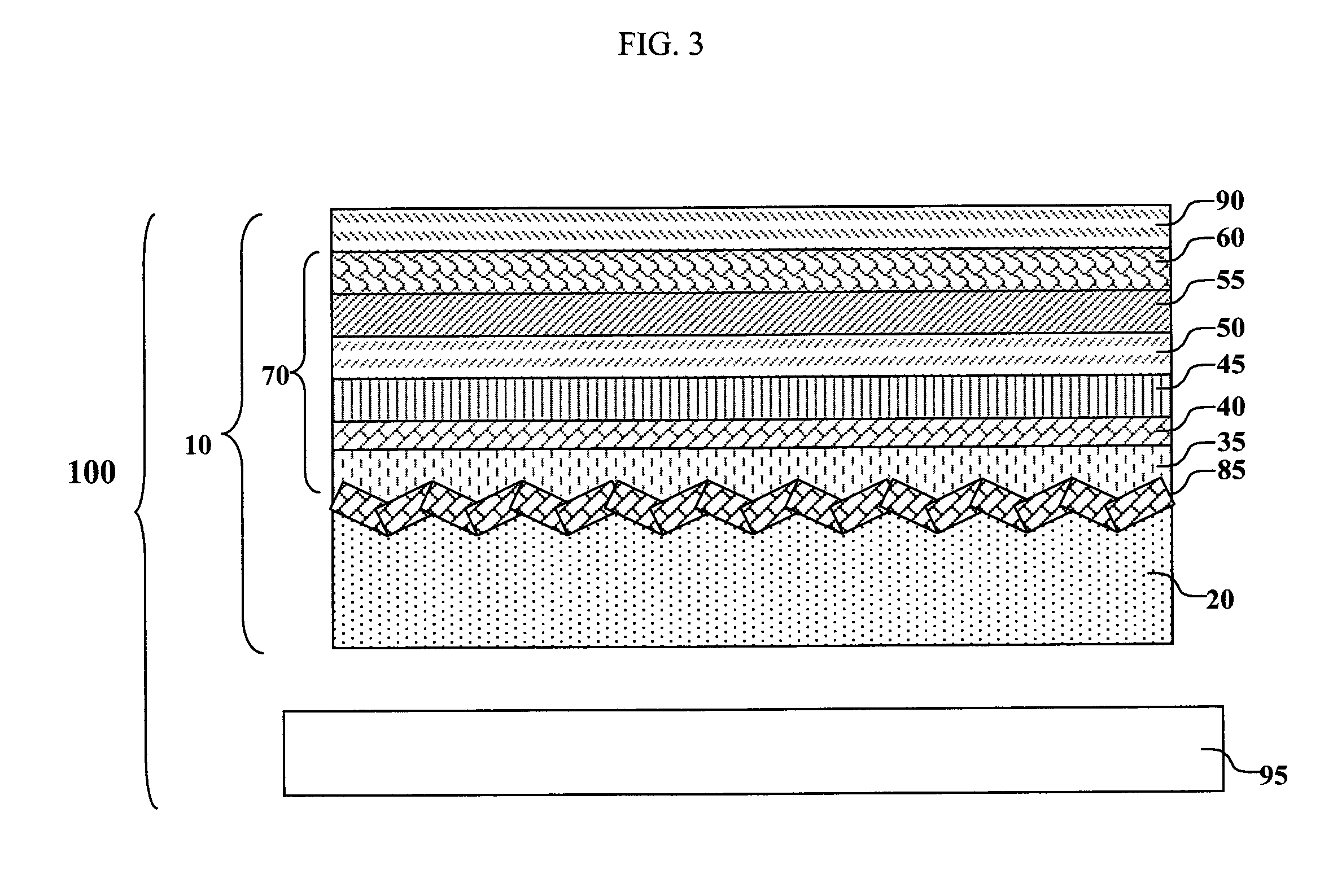
White-emitting microcavity OLED device
a microcavity and electrode technology, applied in the field of white-emitting electroluminescent devices, can solve the problems of insufficient conductivity of such transparent electrodes for applications with much larger individual emitting units, device manufacturing is more difficult, and the control is difficult, etc., to achieve the effect of reducing cost, improving manufacturing ease, and increasing conductivity
- Summary
- Abstract
- Description
- Claims
- Application Information
AI Technical Summary
Benefits of technology
Problems solved by technology
Method used
Image

Examples
example 1 (
CONVENTIONAL OLED—COMPARATIVE)
The preparation of a conventional non-microcavity OLED is as follows: A 1 mm thick glass substrate coated with a transparent ITO conductive layer was cleaned and dried using a commercial glass scrubber tool. The thickness of ITO is about 42 nm and the sheet resistance of the ITO is about 68 Ω / square. The ITO surface was subsequently treated with oxidative plasma to condition the surface as an anode. A 1 nm thick layer of CFx, polymerized fluorocarbon, was deposited on the clean ITO surface as the hole-injecting layer by decomposing CHF3 gas in RF plasma treatment chamber. The substrate was then transferred into a vacuum deposition chamber for deposition of all other layers on top of the substrate. The following layers were deposited in the following sequence by sublimation from a heated boat under a vacuum of approximately 10−6 Torr:
1) a hole transport layer, 107 nm thick, including N,N′-di(naphthalene-1-yl)-N,N′-diphenyl-benzidine (NPB);
2) an elec...
example 2 (
CONVENTIONAL MICROCAVITY OLED DEVICE)
A conventional microcavity OLED was fabricated as follows: A glass substrate was coated with a semitransparent anode layer, 22.5 nm thick, including Ag, by a DC sputtering process at an Ar pressure of about 4 mTorr. A 0.5 nm thick layer of molybdenum oxide, MoO3, was deposited as a hole-injecting layer on the surface of the Ag anode layer in a vacuum chamber using thermal evaporation. The following layers were deposited in the following sequence by sublimation from a heated boat under a vacuum of approximately 10−6 Torr:
1) a hole transport layer, 430 nm thick, including N,N′-di(naphthalene-1-yl)-N,N′-diphenyl-benzidine (NPB);
2) an electron transport layer (also serving as the emissive layer), 70 nm thick, including tris(8-hydroxyquinoline)aluminum(III) (Alq);
3) an electron injection layer, 1 nm thick, including Li; and
4) a cathode, approximately 75 nm thick, including Ag.
After the deposition of these layers, the device was transferred ...
example 3
The comparative microcavity OLED device of Example 2 was used to construct the broadband-emitting OLED apparatus of this example. A piece of 0.125 mm thick Teflon foil was optically attached using vacuum grease to the outside surface of the glass substrate of the microcavity OLED device of Example 2. The resulting output spectra at different angles are shown in FIG. 8. The emission showed little angular dependence and the spectral output resembled that of the Alq emitter as shown in Example 1 and FIG. 6. The total integrated output over all angles is expected to show similar shape and to cover a wide wavelength range from 450 nm to 650 nm. Because of the green Alq organic EL element used in the example, the resulting output was green and not white. The ability of the OLED apparatus to reproduce the spectral output of the emitter, however, clearly demonstrated that a white-emitting OLED apparatus would have resulted if a white emitting organic EL element had been used. In this examp...
PUM
 Abstract
Description
Claims
Application Information