Wet developable hard mask in conjunction with thin photoresist for micro photolithography

a micro-photolithography and hard mask technology, applied in the direction of auxillary/base layers of photosensitive materials, instruments, photosensitive materials, etc., can solve the problems of cumbersome procedure, organic photoresist etching relatively fast, and dof to decreas

Inactive Publication Date: 2005-04-07
BREWER SCI
View PDF19 Cites 41 Cited by
  • Summary
  • Abstract
  • Description
  • Claims
  • Application Information

AI Technical Summary

Benefits of technology

The advanced hard mask and process of the present invention minimize, and more preferably eliminate, the problems described above. In one aspect, the invention is broadly concerned with a method of forming structures to be used in various microelectronic applications such as photolithographic processes for integrated circuit (IC) fabrication and microelectromechanical systems (MEMS) applications.

Problems solved by technology

However, Rayleigh's law also shows that enhancing resolution causes the DOF to decrease.
Unfortunately, organic photoresists etch relatively fast under common hard mask plasma etch chemistries and conditions.
In particular, the procedure is cumbersome, and the patterns for each photoresist layer must be perfectly aligned.

Method used


Image

  • Wet developable hard mask in conjunction with thin photoresist for micro photolithography
  • Wet developable hard mask in conjunction with thin photoresist for micro photolithography
  • Wet developable hard mask in conjunction with thin photoresist for micro photolithography

Examples


example 1

Protective Layer Formulations

1. Preparation of Protective Layer Formulation 1

The ingredients used in this part are set forth in Table 1 below. The diketone ligand (ethyl acetoacetate), chromophore (cyano acrylate), and aminoplast crosslinking agent (Cymel®) were dissolved in one-third of the total solvent (PnP). The mixture was filtered through a membrane filter for ion removal. Then, the polydibutyltitanate and remaining two-thirds of the solvent were added. The final formulation was filtered through a particle filter.

TABLE 1Protective Layer Formulation 1Polydibutyltitanate (obtained from DuPont) 24 gEthyl acetoacetate (obtained from Lonza) 31 gCyano acrylate (obtained from St.-Jean Photochemicals) 6.3 gCymel ® 303LF (obtained from Cytec Industries) 6.3 gPnP (obtained from General Chemical Corp.)332 g

2. Preparation of Protective Layer Formulation 2

The ingredients used in this part are set forth in Table 2 below. The diketone ligand, chromophore, and aminoplast crosslinking...

example 2

Protective Layer Process Conditions

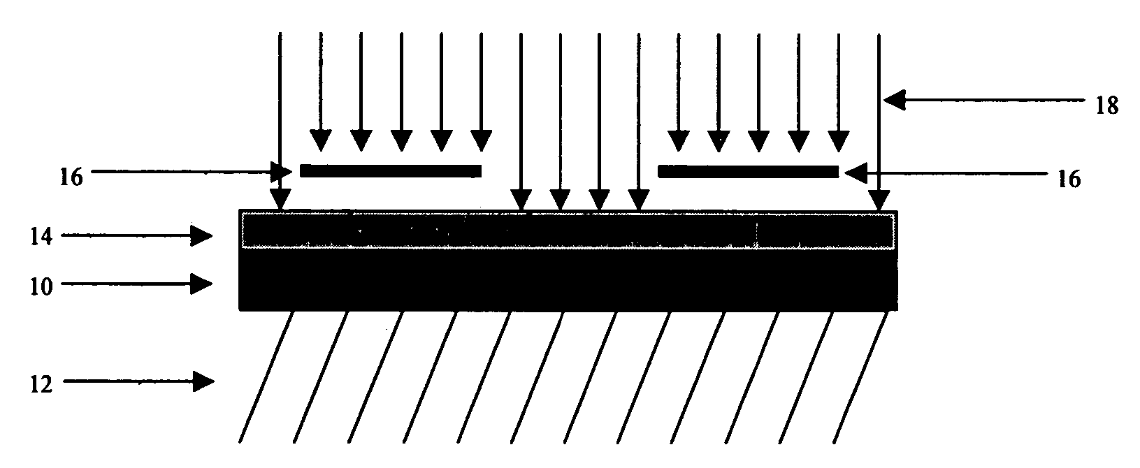
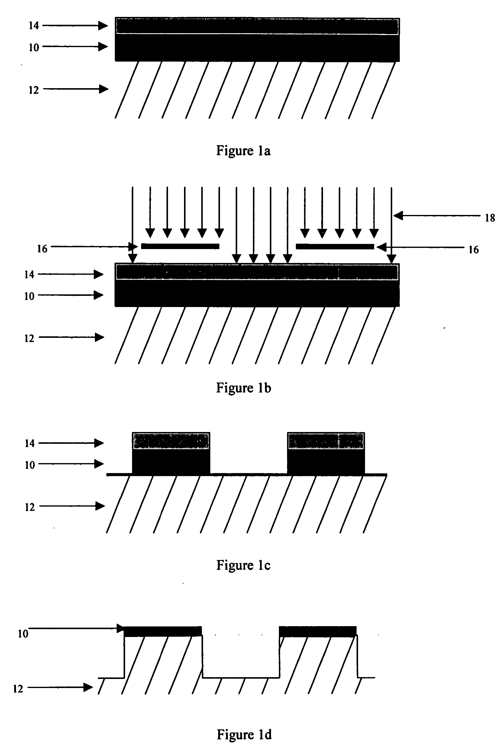
The protective layer formulation prepared in Part 1 of Example 1 was applied to a silicon substrate and processed under the following conditions shown in Table 5.

TABLE 5Process ConditionsSpin speed2000 rpmSpin time 60 secBake temperature 205° C.Bake time 60 sec

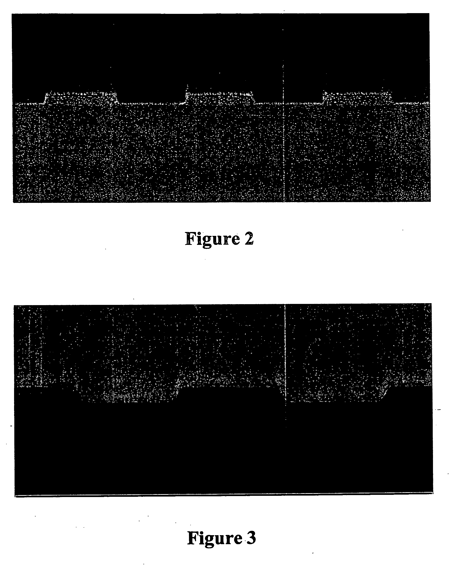
A photoresist (a non-chemically amplified photoresist, sold under the name Ultra i-123 by Shipley) was diluted with ethyl lactate at a weight ratio of 1:6 to achieve a photoresist composition having a solids content of about 2.2% by weight. The photoresist was applied to the protective layer under the following process conditions: 2000 rpm spin coat; 90° C. / 60 sec soft bake; 115° C. / 90 sec post-exposure bake (PEB). FIG. 2 shows cross-sections of dense line patterns (1:1) obtained at 365 nm (exposure dose—110 mJ / cm2) on an i-line stepper (GCA Model 3300, NA 0.43) with the protective layer of this invention and the diluted photoresist thickness. The protective layer thickness was 76 nm. Th...

example 3

Pattern Transfer from Protective Layer to Substrate

The protective layer formulation prepared in Part 1 of Example 1 was applied to the surface of poly silicon. The protective layer was processed with the conditions in Table 5, and yielded a protective layer with a thickness of 75 nm. A photoresist layer was applied on top of the protective layer and was subsequently baked at 90° C. / 60 sec to yield a photoresist layer having a thickness of about 45 nm. The photoresist layer was then exposed through a photomask at a wavelength of 365 nm and baked again at 130° C. / 90 sec. The exposed areas of the protective layer and photoresist were removed by a 0.26 N TMAH solution. Patterns of the protective layer and thin photoresist, similar to the results of Example 2, were obtained. The wafer with line / space patterns of the protective layer on top of 320-nm poly silicon was subjected to reactive ion etch (RE) with following conditions: chlorine (the etchant) 80 sccm; pressure 25 mTorr; and RIE...


PUM

PropertyMeasurementUnit
thicknessaaaaaaaaaa
temperatureaaaaaaaaaa
thicknessaaaaaaaaaa

Abstract

A novel process for using a hard mask or protective layer in conjunction with an extremely thin photoresist is provided. In this process, a thin film of the protective layer is coated on the surface of a substrate that is to be selectively modified by reactive ion etch (RIE). The protective layer is photosensitive and anti-reflective. An extremely thin photoresist layer is coated on top of the protective layer. The stack of the films is selectively exposed to actinic radiation at a wavelength determined by the sensitivities of the protective layer and photoresist layer. The latent images on the photoresist and protective layers resulting from the exposure are developed with a common alkaline developer. The three dimensional patterns of photoresist and underlying protective layer are formed simultaneously by the single exposure and single development. When the underlying substrate is etched by RIE, the protective layer is the masking layer, not the photoresist.

Description

BACKGROUND OF THE INVENTION 1. Field of the Invention The present invention is broadly directed towards new methods of forming microelectronic structures where extremely thin photoresists layers can be utilized. 2. Description of the Prior Art When a photoresist is used to generate patterns by light exposure, Rayleigh's laws can be used to define the pattern resolution and depth of focus (DOF): Resolution=k1λ / NA; and DOF=k2λ / NA2, where λ is the irradiation wavelength, NA is the numerical aperture of the exposure tool, and k1 and k2 are constants for a given process. Rayleigh's theory indicates that an exposure tool with short wavelength and large numerical aperture will produce better pattern resolution. This principle is why the microelectronics industry has been progressively moving toward short exposure wavelengths. However, Rayleigh's law also shows that enhancing resolution causes the DOF to decrease. The use of a thin photoresist decreases the value of k1 and increases t...

Claims


Application Information

Patent Timeline
Patent Type & Authority Applications(United States)
IPC IPC(8): G03C1/492G03C1/494G03C1/76G03C5/00G03F7/00G03F7/09G03F7/095G03F7/11G03F7/30H01LH01L21/308H01L21/31H01L21/3213
CPCG03F7/091G03F7/094H01L21/32139G03F7/11H01L21/3081G03F7/095
Inventor SUN, SAM X.LI, CHENGHONG
Owner BREWER SCI
Why Eureka
Try Eureka