Silicon carbide-oxide layered structure, production method thereof, and semiconductor device

a technology of silicon carbideoxide and layered structure, which is applied in the direction of semiconductor devices, basic electric elements, electrical apparatus, etc., can solve the problems of affecting the application of the above techniques to commercial devices, affecting the actual channel mobility of 20 cm, and affecting the use of commercial devices. , to achieve the effect of high carrier mobility and high electric current drivability

Active Publication Date: 2005-04-14
PANASONIC CORP
View PDF21 Cites 36 Cited by
  • Summary
  • Abstract
  • Description
  • Claims
  • Application Information

AI Technical Summary

Benefits of technology

[0028] A silicon carbide-oxide layered structure or production method thereof according to the present inve...

Problems solved by technology

However, the 4H—SiC (1 1-2 0) substrate is not suitable for mass production and is therefore difficult to be used as a substrate for commercial devices.
However, in a MISFET having a gate insulating film formed of a thermal oxide film according to the above-des...

Method used


Image

  • Silicon carbide-oxide layered structure, production method thereof, and semiconductor device
  • Silicon carbide-oxide layered structure, production method thereof, and semiconductor device
  • Silicon carbide-oxide layered structure, production method thereof, and semiconductor device

Examples


embodiment 1

[0042] (Embodiment 1)

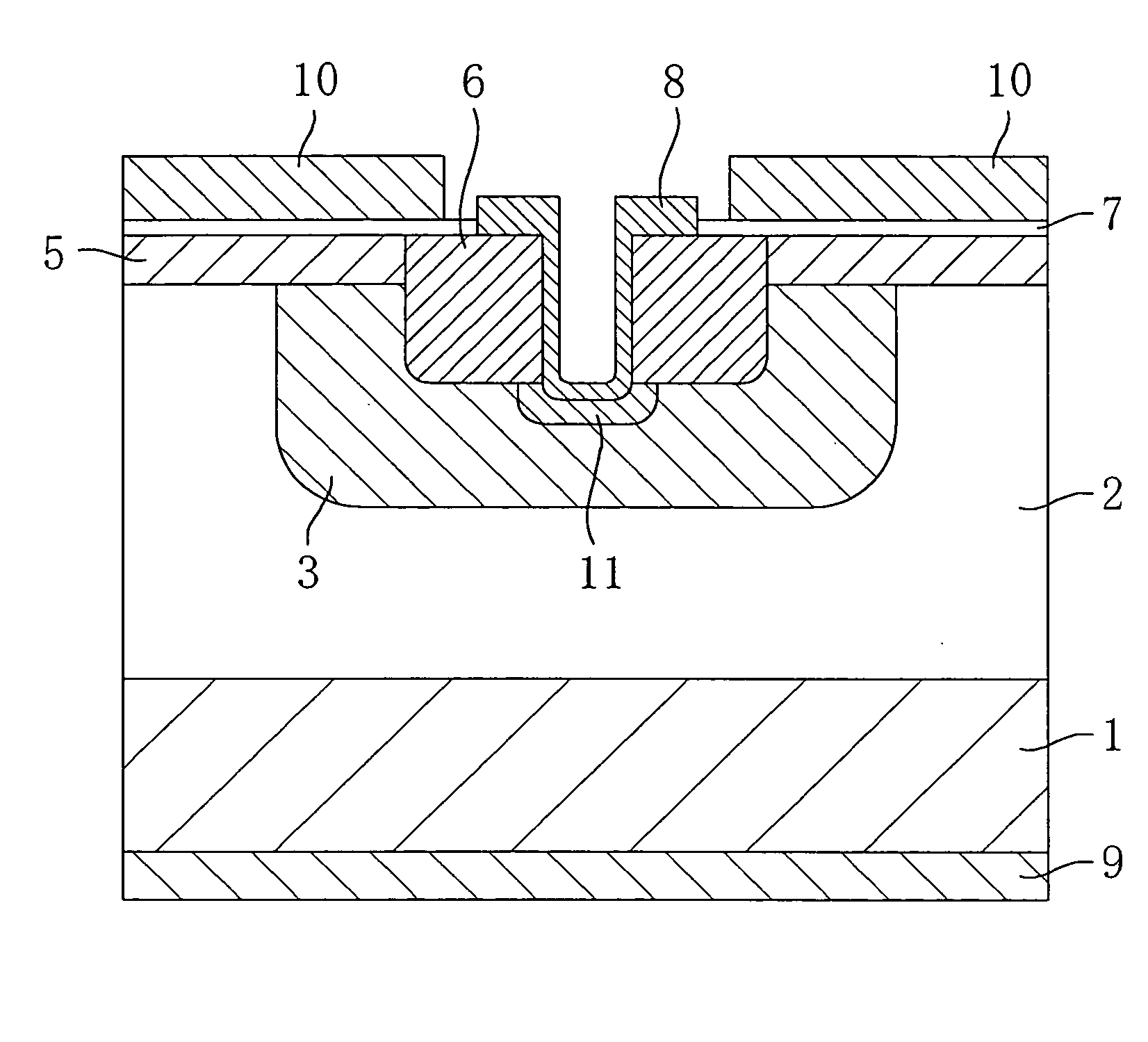
[0043]FIG. 1 is a cross-sectional view showing a structure of an accumulative MISFET which uses a SiC substrate according to embodiment 1 of the present invention. Although only a partial cross section of the structure is shown in FIG. 1, a plan view of the MISFET is as shown in FIG. 2 or FIG. 10 of PCT / JP01 / 07810.

[0044] In embodiment 1, nitrogen is used as a V-group element. However, any other V-group element, such as phosphorus (P), arsenic (As), or the like, may be used.

[0045] In the present invention, a “SiC (silicon carbide) layer” means most preferably a bulk monocrystalline SiC substrate or a SiC layer epitaxially grown on a bulk monocrystalline SiC substrate. SiC has many polytypes, among which 3C, 4H, 6H and 15R polytypes are especially useful for electronic devices. When these polytypes are used, the present invention brings adequate results. In the description provided below, the SiC layer is a 4H—SiC (0 0 0 1) layer epitaxially grown on a bulk SiC ...

embodiment 2

[0090] (Embodiment 2)

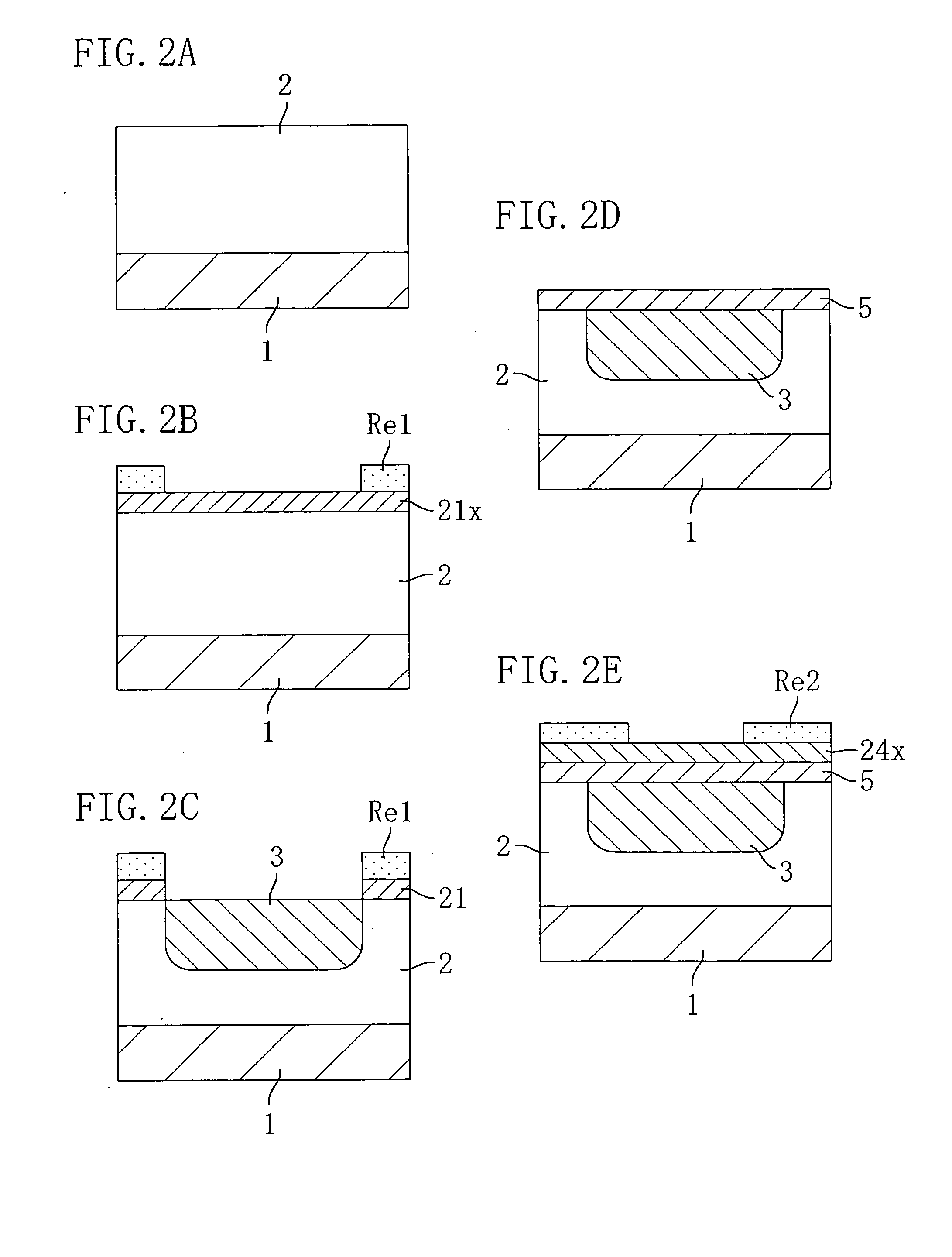
[0091] In embodiment 2, the structure of a silicon carbide-oxide layered structure is basically the same as that of embodiment 1, and therefore, the description thereof is herein omitted. Only the production process of embodiment 2 is described in this section.

[0092] In embodiment 2, a first oxide layer is formed over the surface of the SiC layer before the step of FIG. 4B. The thickness of the first oxide layer is preferably smaller than 20 nm, e.g., about 8 nm. Thereafter, the structure is annealed in an inert gas (Ar, N2, He, Ne, or the like) atmosphere at 1000° C. or higher (e.g., 1000° C. to 1150° C.). The first oxide layer is densified in advance by this annealing treatment.

[0093] Then, the structure is annealed for 1 hour with a gas containing nitrogen, such as NO gas, N2O gas, or the like, or a gas containing phosphorus (P), for example, at 1150° C. with a chamber internal pressure of 150 Torr (about 2.00×10⁴ Pa).

[0094] Then, a second oxide layer havi...


PUM


Abstract

A gate insulating film which is an oxide layer mainly made of SiO2 is formed over a silicon carbide substrate by thermal oxidation, and then, a resultant structure is annealed in an inert gas atmosphere in a chamber. Thereafter, the silicon carbide-oxide layered structure is placed in a chamber which has a vacuum pump and exposed to a reduced pressure NO gas atmosphere at a high temperature higher than 1100° C. and lower than 1250° C., whereby nitrogen is diffused in the gate insulating film. As a result, a gate insulating film which is a V-group element containing oxide layer, the lower part of which includes a high nitrogen concentration region, and the relative dielectric constant of which is 3.0 or higher, is obtained. The interface state density of an interface region between the V-group element containing oxide layer and the silicon carbide layer decreases.

Description

CROSS-REFERENCE TO RELATED APPLICATION [0001] This application claims priority under 35 U.S.C. §119(a) on Japanese Patent Application No. 2003-350244 filed on Oct. 9, 2003, the entire contents of which are hereby incorporated by reference.BACKGROUND OF THE INVENTION [0002] The present invention relates to a silicon carbide-oxide layered structure including a silicon carbide layer, a production method thereof, and a semiconductor device produced by using the silicon carbide-oxide layered structure. [0003] In recent years, applications of silicon carbide (SiC) to low-loss power devices have been expected because silicon carbide has a structure where Si and C are bonded at the composition ratio of 1:1 and has high breakdown tolerance as compared with other wide band gap semiconductor materials. [0004] One of the most practicable applications of SiC to a power device is the application to a SiC device for power driving which has an insulated-gate transistor, i.e., a SiC-MISFET structure...

Claims


Application Information

Patent Timeline
IPC IPC(8): H01L21/04H01L29/24H01L29/417H01L29/51H01L29/78
CPCH01L29/7828H01L21/049H01L29/1608H01L29/7827H01L29/513H01L29/518H01L29/66068H01L29/41766
Inventor YAMASHITA, KENYAKITABATAKE, MAKOTOKUSUMOTO, OSAMUTAKAHASHI, KUNIMASAUCHIDA, MASAOMIYANAGA, RYOKO
Owner PANASONIC CORP
Why Eureka
Try Eureka