Device including an amorphous carbon layer for improved adhesion of organic layers and method of fabrication

a technology of organic layer and carbon layer, applied in the field of semiconductor processing techniques, can solve the problems of reduced photolithography quality, poor adhesion of low surface energy materials to a substrate surface, and poor adhesion of materials with low surface energy to a substrate surface, and achieve the effect of improving chemical vapor deposition

Active Publication Date: 2005-04-14
NXP USA INC
View PDF3 Cites 19 Cited by
  • Summary
  • Abstract
  • Description
  • Claims
  • Application Information

AI Technical Summary

Benefits of technology

[0012] These needs and others are substantially met through provision of a device and a method of fabricating the device including a substrate, a low surface energy material layer, and an amorphous carbon layer disposed overlying the substrate and adjacent the low surface energy material layer. The method of fabricating the device includes the steps of providing a substrate having a surface, depositing a low surface energy material layer overlying the substrate, and depositing an amorphous carbon layer overlying the surface of the substrate, but adjacent the low surface energy material layer. The amorphous carbon layer is formed utilizing standard plasma enhanced chemical vapor deposition techniques (PECVD) or by sputtering.

Problems solved by technology

Organic material layer adhesion, in the form of photoresist adhesion, to substrates having a layer of low surface energy material such as Teflon AF® present on the surface, and the adhesion of low surface energy materials to a substrate surface, is very poor using current methodology.
The result is a reduction in the quality of photolithography processing, and the inability to incorporate low surface energy materials into the layers of a multi-layer device.
While many surface pretreatment options have been utilized, these conventional procedures have failed to demonstrate the adhesive durability required to complete all necessary processing steps.
However, none of these processes has improved adhesion adequately.
However, HMDS is only chemically compatible with silicon and its oxides and does not react in the same manner with most other materials.
It has additionally been found that traditional vapor priming lasts only three days until the wafers must be primed again.
This is objectionable for certain temperature sensitive applications, and as previously stated, vapor priming with HMDS has no effect on most low surface energy materials such as Teflon or other fluoropolymers.
However, such coatings must be later removed which can present additional problems.
For example, it has been found that removal of the SiN material, generally through dry etching techniques, is very aggressive and can lead to damage of a fragile wafer epi layer.
This process temporarily raises surface energy, but results in only a transient effect since low surface energy functional groups in the molecule re-migrate to the surface restoring its original low level of energy.
In addition, the surface roughness remains which may not be desirable.
The process is complicated and requires double resist coats since wetting by the first coating usually remains incomplete.
Aluminum has been used, yet aluminum etches in the resist developer, thereby limiting resolution.

Method used


Image

  • Device including an amorphous carbon layer for improved adhesion of organic layers and method of fabrication
  • Device including an amorphous carbon layer for improved adhesion of organic layers and method of fabrication
  • Device including an amorphous carbon layer for improved adhesion of organic layers and method of fabrication

Examples


Embodiment Construction

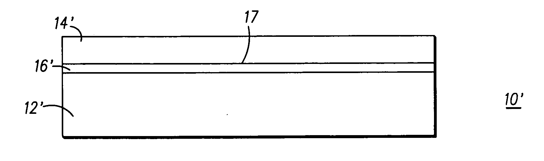
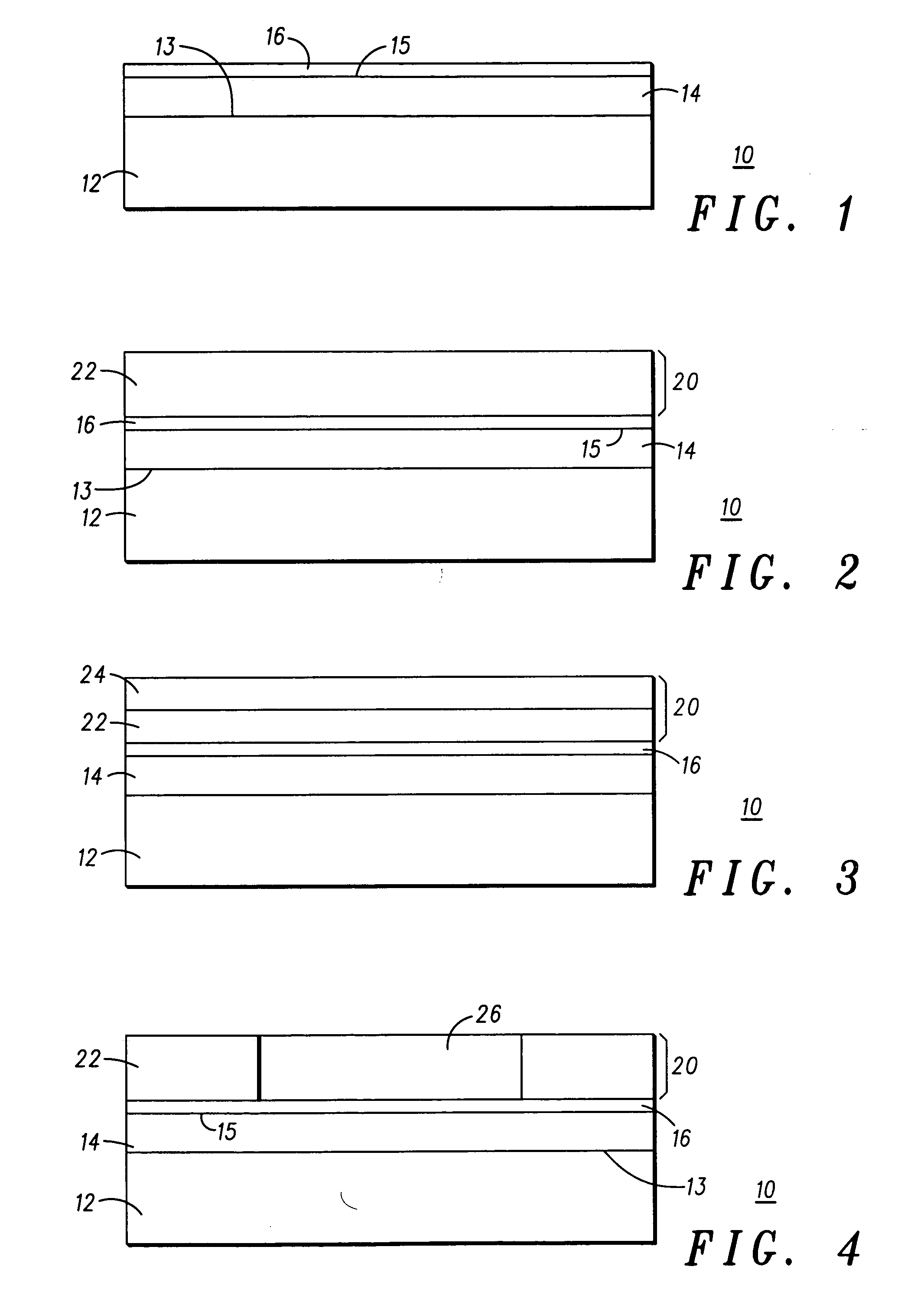
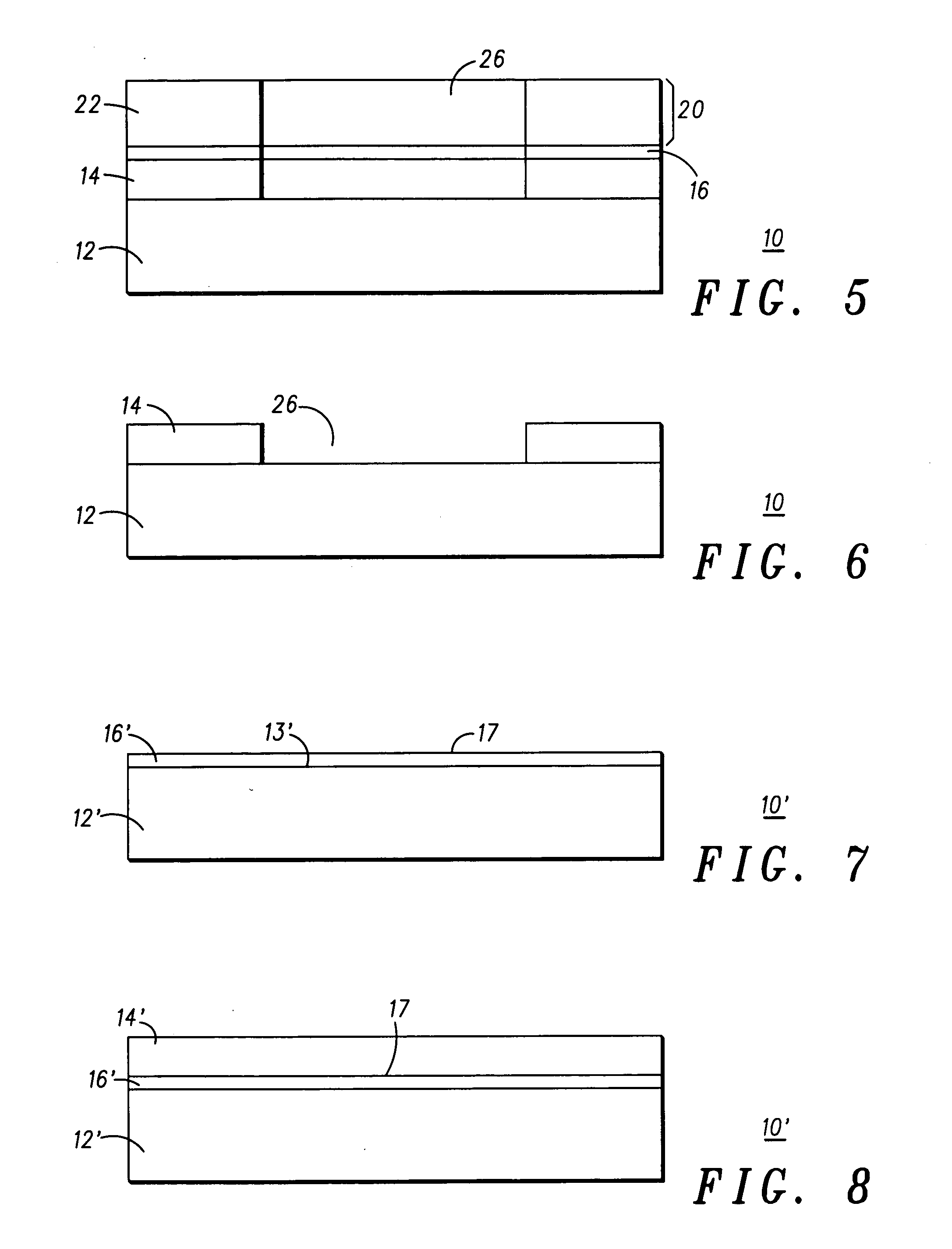
[0016] During the course of this description, like numbers are used to identify like elements according to the different figures that illustrate the invention. In addition, during the course of the description of the preferred embodiments, a semiconductor device is described, yet it is anticipated by this disclosure that the term “device” may include a semiconductor device, a photonic device, a microfluidic device, an acoustic wave device, an imprint template, or the like. Accordingly, FIG. 1 illustrates in simplified cross-sectional view a first step in the method of fabricating a device, namely a semiconductor device, according to the present invention. Illustrated in FIG. 1 is a semiconductor device, generally referenced 10, including as a first step the providing of a substrate 12. In this particular embodiment, substrate 12 is described as being formed of silicon or a silicon oxide material. More specifically, substrate 12 is described as being formed of silicon. It should be u...


PUM

PropertyMeasurementUnit
contact angleaaaaaaaaaa
temperatureaaaaaaaaaa
densityaaaaaaaaaa

Abstract

A novel device, such as a semiconductor device, a microfluidic device, a surface acoustic wave device an imprint template, or the like, including an amorphous carbon layer for improved adhesion of organic layers and method of fabrication. The device includes a substrate having a surface, an amorphous carbon layer, formed overlying the surface of the substrate, and a low surface energy material layer overlying the surface of the substrate. The device is formed by providing a substrate having a surface, depositing a low surface energy material layer and an amorphous carbon layer overlying the surface of the substrate adjacent the low surface energy material layer using plasma enhanced chemical vapor deposition (PECVD) or sputtering.

Description

FIELD OF THE INVENTION [0001] The present invention relates to semiconductor processing techniques, and more particularly to an electronic device, such as a semiconductor device, having improved adhesion qualities and a method for fabricating the device including enhanced adhesion of organic layers. BACKGROUND OF THE INVENTION [0002] Organic material layer adhesion, in the form of photoresist adhesion, to substrates having a layer of low surface energy material such as Teflon AF® present on the surface, and the adhesion of low surface energy materials to a substrate surface, is very poor using current methodology. The result is a reduction in the quality of photolithography processing, and the inability to incorporate low surface energy materials into the layers of a multi-layer device. There have been several attempts to improve the adhesion of organic materials, such as photoresists, to the surface of various substrates having as a top surface a low surface energy material present...

Claims


Application Information

Patent Timeline
Patent Type & Authority Applications(United States)
IPC IPC(8): G03F7/09H01LH01L21/00H01L23/48H01L23/52H01L29/22H01L29/40
CPCB82Y10/00G03F7/094G03F7/09
Inventor MANCINI, DAVID P.QUINTERO, JAIME A.RESNICK, DOUG J.SMITH, STEVEN M.
Owner NXP USA INC
Why Eureka
Try Eureka