Methods of forming power semiconductor devices using boule-grown silicon carbide drift layers and power semiconductor devices formed thereby

a technology of silicon carbide and power semiconductor, which is applied in the direction of crystal growth process, polycrystalline material growth, chemistry apparatus and processes, etc., can solve the problem of devices having a characteristic minority carrier lifetime in excess of 50 nanoseconds, and achieve high doping

Active Publication Date: 2005-04-21
CREE INC
View PDF28 Cites 72 Cited by
  • Summary
  • Abstract
  • Description
  • Claims
  • Application Information

AI Technical Summary

Benefits of technology

[0008] According to still further embodiments of the present invention, a silicon carbide junction field effect transistor (JFET) may be formed by forming a 4H boule-grown silicon carbide drift layer having a net n-type dopant concentration therein in a range from between about 2×1014 cm−3 and about 2×1015 cm−3 and then forming an n-type silicon carbide epilayer on a Si-face of the silicon carbide drift layer. This n-type epilayer operates as the channel region of the JFET. An n-type silicon carbide source region is formed on or within the n-type silicon carbide epilayer. The n-type source region is more highly doped than the n-type epilayer and the n-type epilayer is more highly doped than the n-type drift layer. A p-type silicon carbide gate electrode is formed on the n-type silicon carbide epilayer so that a p-n rectifying junction is defined therebetween. When reversed biased, this p-n rectifying junction operates to deplete the n-type epilayer of majority carriers and block a forward on-state conduction path between the n-type source region and the n-type drift layer. This forward on-state conduction path may extend through an opening in a p-type silicon carbide buried region, which extends between the n-type epilayer and the n-type drift layer. In particular, a p-type silicon carbide buried region may be formed adjacent a Si-face of the drift layer prior to forming the n-type epilayer.

Problems solved by technology

In particular, the use of high purity silicon carbide wafer material in minority carrier devices may result in devices having a characteristic minority carrier lifetime in excess of 50 nanoseconds.

Method used


Image

  • Methods of forming power semiconductor devices using boule-grown silicon carbide drift layers and power semiconductor devices formed thereby
  • Methods of forming power semiconductor devices using boule-grown silicon carbide drift layers and power semiconductor devices formed thereby
  • Methods of forming power semiconductor devices using boule-grown silicon carbide drift layers and power semiconductor devices formed thereby

Examples


Embodiment Construction

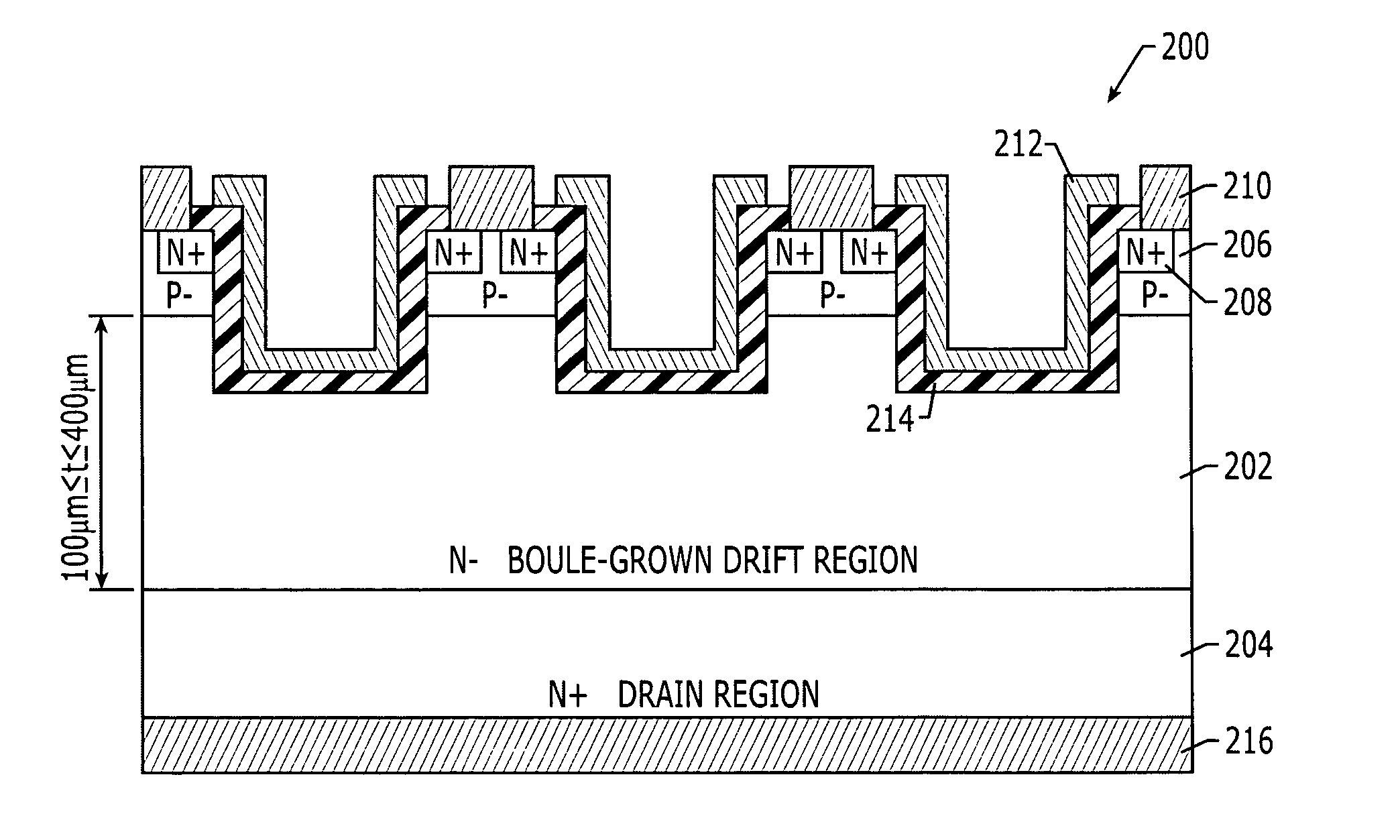
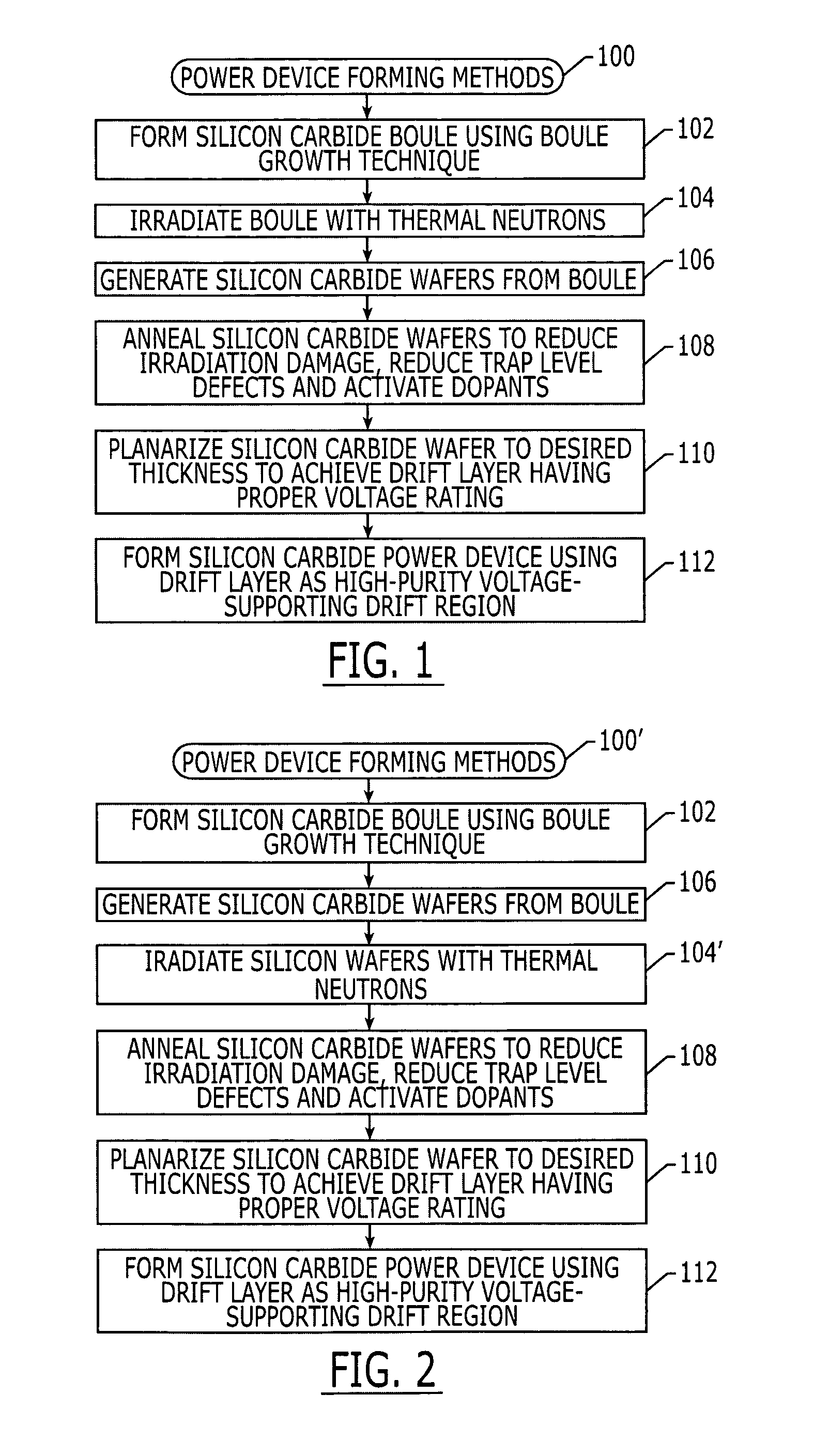
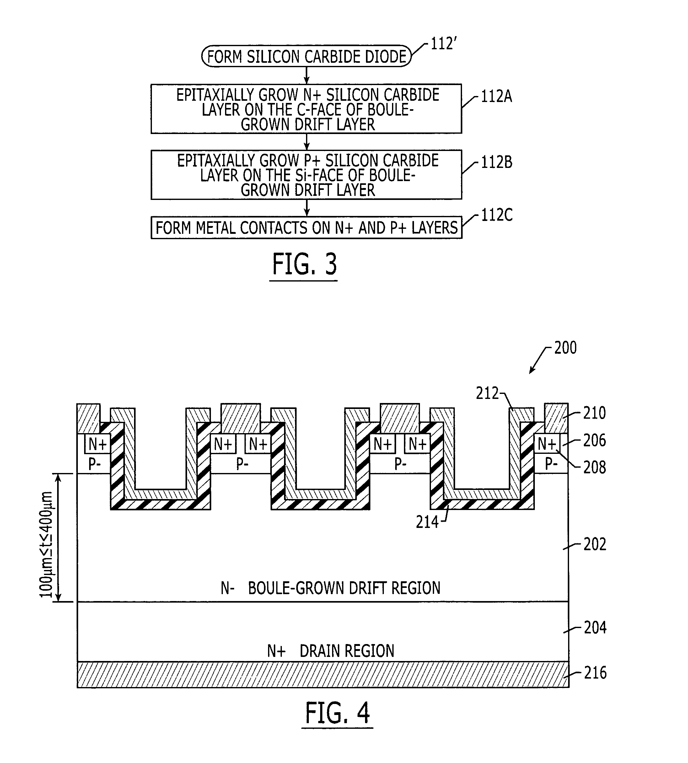
[0015] The present invention will now be described more fully hereinafter with reference to the accompanying drawings, in which embodiments of the invention are shown. This invention may, however, be embodied in different forms and should not be construed as limited to the embodiments set forth herein. Rather, these embodiments are provided so that this disclosure will be thorough and complete, and will fully convey the scope of the invention to those skilled in the art. In the drawings, the thickness of layers and regions are exaggerated for clarity. It will also be understood that when a layer is referred to as being “on” another layer or substrate, it can be directly on the other layer or substrate, or intervening layers may also be present. Moreover, the terms “first conductivity type” and “second conductivity type” refer to opposite conductivity types such as N or p-type, however, each embodiment described and illustrated herein includes its complementary embodiment as well. Th...


PUM

PropertyMeasurementUnit
blocking voltage ratingaaaaaaaaaa
thicknessaaaaaaaaaa
thicknessaaaaaaaaaa

Abstract

Methods of forming high voltage silicon carbide power devices utilize high purity silicon carbide drift layers that are derived from high purity silicon carbide wafer material, instead of prohibitively costly epitaxially grown silicon carbide layers. The methods include forming both minority carrier and majority carrier power devices that can support greater than 10 kV blocking voltages, using drift layers having thicknesses greater than about 100 um. The drift layers are formed as boule-grown silicon carbide drift layers having a net n-type dopant concentration therein that is less than about 2×1015 cm−3. These n-type dopant concentrations can be achieved using neutron transmutation doping (NTD) techniques.

Description

FIELD OF THE INVENTION [0001] The present invention relates to semiconductor device fabrication methods, and more particularly to methods of forming silicon carbide power devices and devices formed thereby. BACKGROUND OF THE INVENTION [0002] Semiconductor power devices are widely used to carry large currents and support high voltages. Conventional power devices are generally fabricated using silicon semiconductor material. One widely used power device is the power MOSFET. In a power MOSFET, a gate electrode provides turn-on and turn-off control upon the application of an appropriate gate bias. For example, turn-on in an n-type enhancement-mode MOSFET occurs when a conductive n-type inversion-layer channel (also referred to as “channel region”) is formed in a p-type base region in response to application of a positive gate bias. The inversion-layer channel electrically connects the n-type source and drift / drain regions and allows for majority carrier conduction therebetween. [0003] T...

Claims


Application Information

Patent Timeline
Patent Type & Authority Applications(United States)
IPC IPC(8): C30B29/36C30B31/20H01L21/04H01L29/24H01L29/739H01L29/78H01L29/808H01L29/861H01L29/868H01L31/0312
CPCC30B29/36C30B31/20H01L21/0455H01L29/6606H01L29/868H01L29/7813H01L29/8083H01L29/861H01L29/66068H01L29/00
Inventor SUMAKERIS, JOSEPH JOHNHOBGOOD, HUDSON MCDONALDPAISLEY, MICHAEL JAMESJENNY, JASON RONALDCARTER, CALVIN H. JR.TSVETKOV, VALERI FEDOROVICH
Owner CREE INC
Why Eureka
Try Eureka