Non-volatile memory technology suitable for flash and byte operation application

a non-volatile memory and byte operation technology, applied in the field of non-volatile memory cells, can solve the problems of non-uniform erase thresholds, start to erase memory cells, and holes generated by band-to-band tunneling trapped in gate oxides, etc., and achieve the effect of reducing die siz

Active Publication Date: 2005-04-21
MARLIN SEMICON LTD
View PDF7 Cites 28 Cited by
  • Summary
  • Abstract
  • Description
  • Claims
  • Application Information

AI Technical Summary

Benefits of technology

[0017] It is one object of the present invention to provide a cell structure, which can compatibly for flash memory cell and EEPROM cell (electrically erasable programmable reads only memory) applications to reduce the die size.

Problems solved by technology

If the substrate current is sufficiently high, the hot holes that are generated by the breakdown may start to erase the memory cell.
Additionally, some holes that are generated by band-to-band tunneling are trapped in the gate oxide.
This may lead to erase threshold non-uniformity, speed-up pf erase time with cycling, degradation of charge retention, or speed-up of gate disturb.
Offsetting the expected improvement in erase performance is the additional circuit complexity that is required for the switching of both positive and negative voltages by the word-line driver circuit.

Method used


Image

  • Non-volatile memory technology suitable for flash and byte operation application
  • Non-volatile memory technology suitable for flash and byte operation application
  • Non-volatile memory technology suitable for flash and byte operation application

Examples


Embodiment Construction

[0029] Some sample embodiments of the invention will now be described in greater detail. Nevertheless, it should be recognized that the present invention can be practiced in a wide range of other embodiments besides those explicitly described, and the scope of the present invention is expressly not limited except as specified in the accompanying claims.

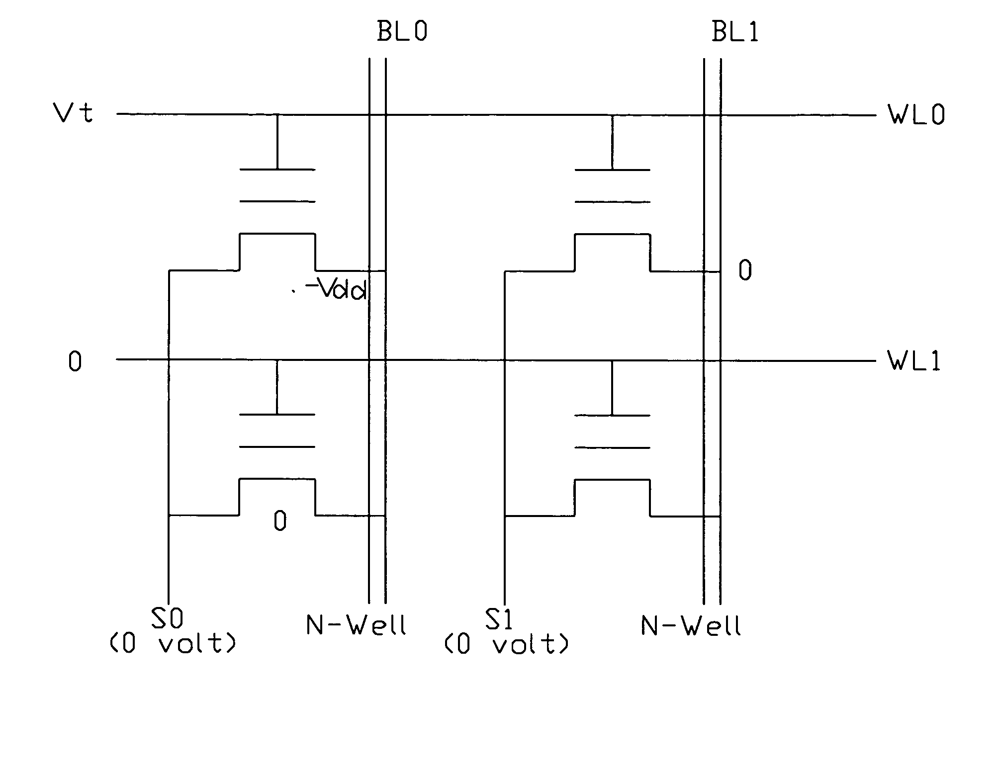
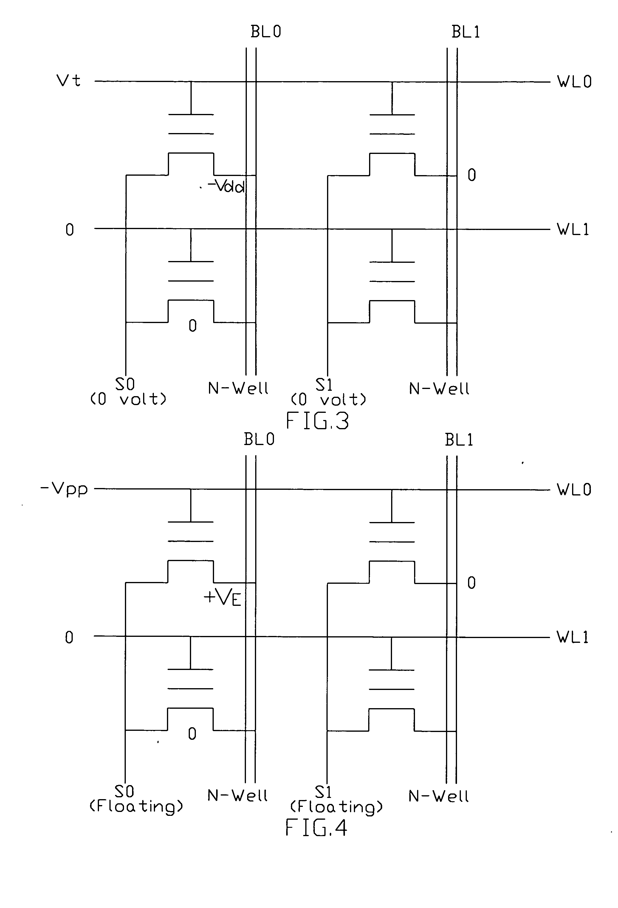
[0030] The present invention provides a P-channel non-volatile memory cell that is invented to fit both the byte operation and flash operation in the same chip for the system on chip (SOC) era. Therefore, the present invention provides a flash memory cell only utilized one transistor to perform the byte operation by using P-channel non-volatile memory cell so as to the space of the memory cell can be reduced and the complex process can be simplified, and the cost can be greatly decreased.

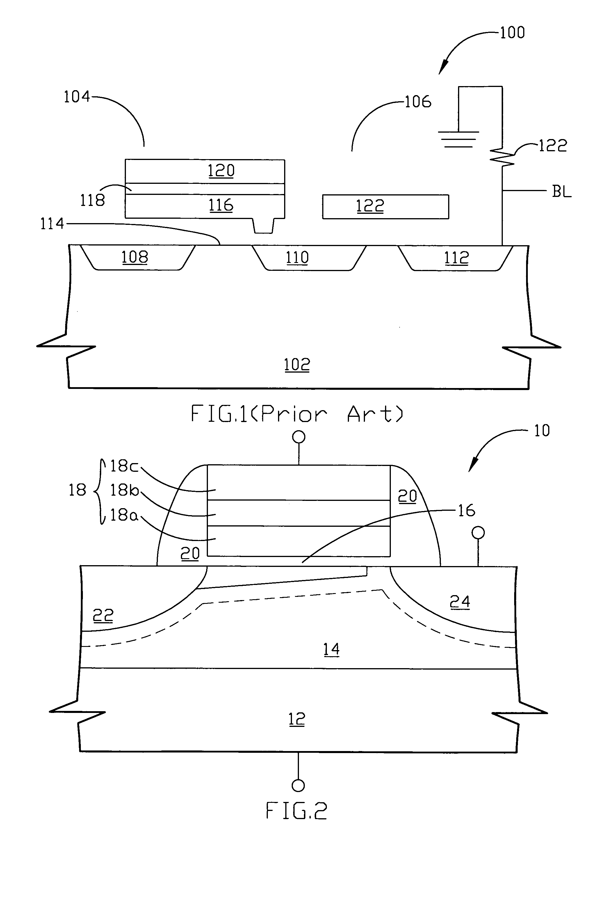
[0031] Referring to FIG. 2, the present invention provides a flash memory cell 10 with one transistor, which includes a P-type substrate 12 and an ...


PUM


Abstract

The present invention provides a non-volatile memory cell structure suitable for the flash memory cell and EEPROM cell (electrically erasable programmable read only memory cell) to perform the byte programming and byte erase operations. In the programming operation, a higher negative voltage applied to the drain region, such that the hot hole is generated to induce the hot electron into the floating gate through the tunneling oxide layer in the lateral electrical field. In addition, the gate voltage is around the threshold voltage, which dependent on the integration circuit device design. Furthermore, the non-volatile memory cell utilized the channel Fowler-Nordheim tunneling for erasing operation. In order to perform the byte erasing operation, the drain junction used as an inhibition switch. Thus, the unselected cell in the same word line is inhibited by biasing the drain to ground. Therefore, the word lines of unselected cells are ground.

Description

BACKGROUND OF THE INVENTION [0001] 1. Field of the Invention [0002] The present invention generally relates to a non-volatile memory cell with its operations, and more particularly to a non-volatile memory cell suitable for flash and byte operation application. [0003] 2. Description of the Prior Art [0004] Semiconductor based memory devices largely comprises Random Access Memories (RAM) and Read Only Memory (ROM). RAM is referred to as volatile memory, in that when supply voltage is removed, data is destroyed with the passage of time. ROM devices, including Programmable ROM (PROM), Erasable PROM (EPROM), and Electrically EPROM (EEPROM). Numerous EEPROM cells and flash memory cells can be simultaneously erased, and are characterized by a stacked gate structure comprising a floating gate and a control gate. [0005] The conventional P-channel stacked gate flash cell programming operation is utilized the channel hot hole induces the hot electron to put the electron into the floating gate...

Claims


Application Information

Patent Timeline
Patent Type & Authority Applications(United States)
IPC IPC(8): G11C8/08G11C16/08G11C16/16
CPCG11C8/08G11C16/16G11C16/08
Inventor HUANG, CHIH-JEN
Owner MARLIN SEMICON LTD
Why Eureka
Try Eureka