Attenuated phase shift mask for extreme ultraviolet lithography and method therefore

a phase shift mask and ultraviolet radiation technology, applied in the field of semiconductor integrated circuit fabrication, can solve the problems of inability to extend the process indefinitely, radiation having a wavelength below 157 nanometers is readily absorbed by most materials including quartz, and the resolution and depth of focus of the optical system become more of an issu

Active Publication Date: 2005-04-21
NXP USA INC
View PDF10 Cites 44 Cited by
  • Summary
  • Abstract
  • Description
  • Claims
  • Application Information

AI Technical Summary

Problems solved by technology

The semiconductor industry has had exceptional success in refining the simple chrome masking process to produce smaller geometry devices using smaller wavelengths of radiation but the process cannot be extended indefinitely.
The problem is that radiation having a wavelength below 157 nanometers is readily absorbed by most materials including quartz.
Furthermore, the resolution and depth of focus of an optical system become more of an issue at the smaller wavelengths when using a conventional lithographic approach.
Also, diffraction effects are a problem in producing sharp delineation between areas on a semiconductor wafer surface receiving and not receiving EUV light.

Method used


Image

  • Attenuated phase shift mask for extreme ultraviolet lithography and method therefore
  • Attenuated phase shift mask for extreme ultraviolet lithography and method therefore
  • Attenuated phase shift mask for extreme ultraviolet lithography and method therefore

Examples


Embodiment Construction

[0017] The following detailed description is merely exemplary in nature and is not intended to limit the invention or the application and uses of the invention. Furthermore, there is no intention to be bound by any expressed or implied theory presented in the preceding technical field, background, brief summary or the following detailed description.

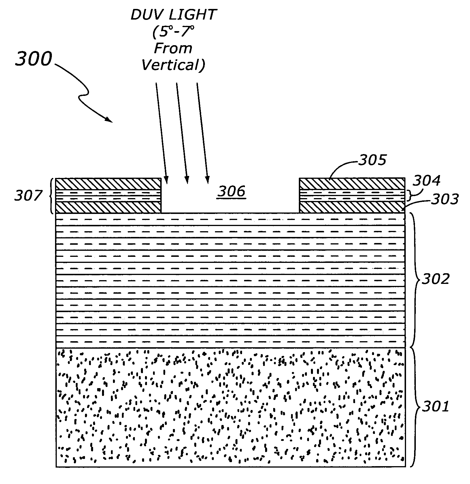
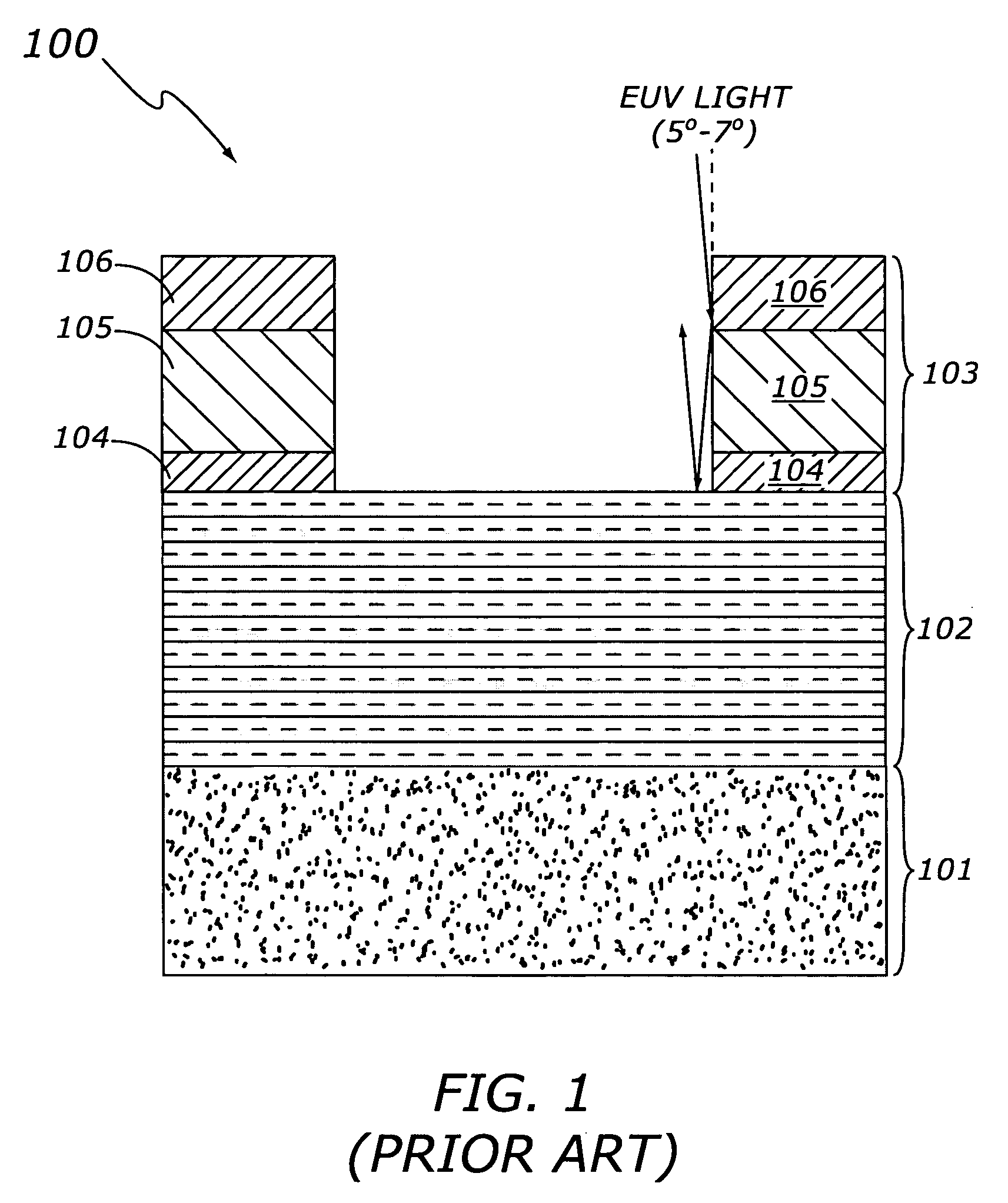
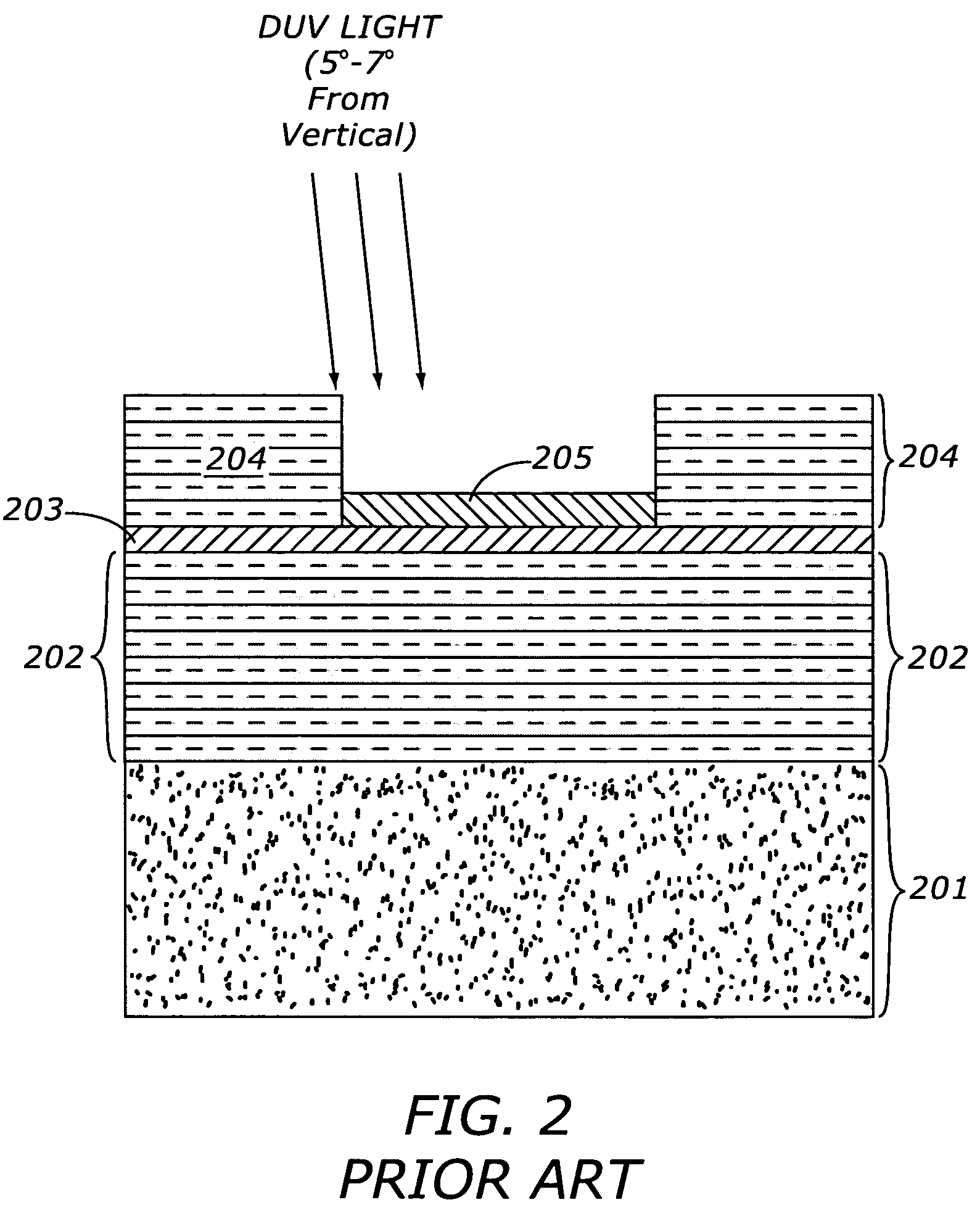
[0018]FIG. 1 is an illustration of a prior art phase shift mask 100 for extreme ultra violet (EUV) lithography. Phase shift mask 100 comprises a substrate 101, a reflectance region 102, and an absorber stack 103. Substrate 101 is a support structure for phase shift mask 100 and is a platform for the layers that comprise the structure. The primary material for substrate 101 is an ultra low thermal expansion material (LTEM). Quartz is not transmissive to extreme ultra violet radiation. EUV radiation does not pass through phase shift mask 100 but is reflected to a semiconductor wafer to expose a layer of photoresist that is deposited on a s...


PUM

PropertyMeasurementUnit
heightaaaaaaaaaa
thickaaaaaaaaaa
wavelengthaaaaaaaaaa

Abstract

Methods and apparatus are provided for extreme ultraviolet phase shift masks. The apparatus comprises a substrate, a reflectance region, and an attenuating phase shifter. The reflectance region overlies the substrate. The attenuating phase shifter overlies the reflectance region. The attenuating phase shifter includes a plurality of openings that expose portions of the reflectance region. The attenuating phase shifter attenuates radiation through a combination of absorption and destructive interference. The method comprises projecting radiation having a wavelength less than 40 nanometers towards a mask having a plurality of openings through an attenuating phase shifter. The plurality of openings expose a reflectance region in the mask. The attenuating phase shifter is less than 700 angstroms thick. Radiation impinging on the reflectance region exposed by said plurality of openings is reflected whereas radiation impinging on the attenuating phase shifter is attenuated and shifted in phase. The attenuating phase shifter attenuates using absorption and destructive interference.

Description

TECHNICAL FIELD OF THE INVENTION [0001] The present invention generally relates to the fabrication of semiconductor integrated circuits, and more particularly relates to phase shift masks using extreme ultraviolet radiation. BACKGROUND OF THE INVENTION [0002] An optical mask is used to pattern a photoresist layer on a semiconductor substrate. The patterned photoresist layer on the semiconductor substrate forms a mask that is used in conjunction with wafer processing techniques to form devices and interconnect of an integrated circuit. The optical masking process that has dominated wafer processing for the past several decades comprises a quartz substrate patterned with a chrome layer. The optical mask is projection aligned to the semiconductor wafer and is optically reduced, typically in a 4:1 ratio. Radiation of a predetermined wavelength is projected through the mask. The predetermined wavelength is selected such that it passes through the quartz substrate readily. Chromed areas o...

Claims


Application Information

Patent Timeline
Patent Type & Authority Applications(United States)
IPC IPC(8): G03C5/00G03F1/00G03F1/14G03F9/00G21K1/06G21K5/00
CPCB82Y10/00B82Y40/00G21K1/062G03F1/32G03F1/24
Inventor HAN, SANG-INHECTOR, SCOTT D.MANGAT, PAWITTER
Owner NXP USA INC
Why Eureka
Try Eureka