Dual capacitor structure for imagers and method of formation

a capacitor and imager technology, applied in the direction of diodes, semiconductor devices, radiation controlled devices, etc., can solve the problems of high power dissipation of large arrays, ccd imagers suffer from a large number, and high leakage, and achieve high capacitance and low leakage

Active Publication Date: 2005-04-28
APTINA IMAGING CORP
View PDF6 Cites 9 Cited by
  • Summary
  • Abstract
  • Description
  • Claims
  • Application Information

AI Technical Summary

Benefits of technology

[0008] The present invention provides imaging devices comprising in-pixel and peripheral capacitors. The capacitors used in peripheral circuits have different requirements from the in-pixel or active capacitors. In one embodiment, dual stack capacitors comprising two dielectric layers may be provided in both the active pixel area and the peripheral area to achieve low leakage and high capacitance. In another embodiment, a dual dielectric capacitor may be provided in one of the active or the peripheral areas, and a single dielectric capacitor is provided in the

Problems solved by technology

However, CCD imagers suffer from a number of disadvantages.
For example, they are susceptible to radiation damage, they exhibit destructive read out over time, they require good light shielding to avoid image smear and they have a high power dissipation for large arrays.
As a result of the inability of the capacitors to fully collect and store the electric charge collected by the photosensitive area, conventional imagers typically suffer f

Method used


Image

  • Dual capacitor structure for imagers and method of formation
  • Dual capacitor structure for imagers and method of formation
  • Dual capacitor structure for imagers and method of formation

Examples


Embodiment Construction

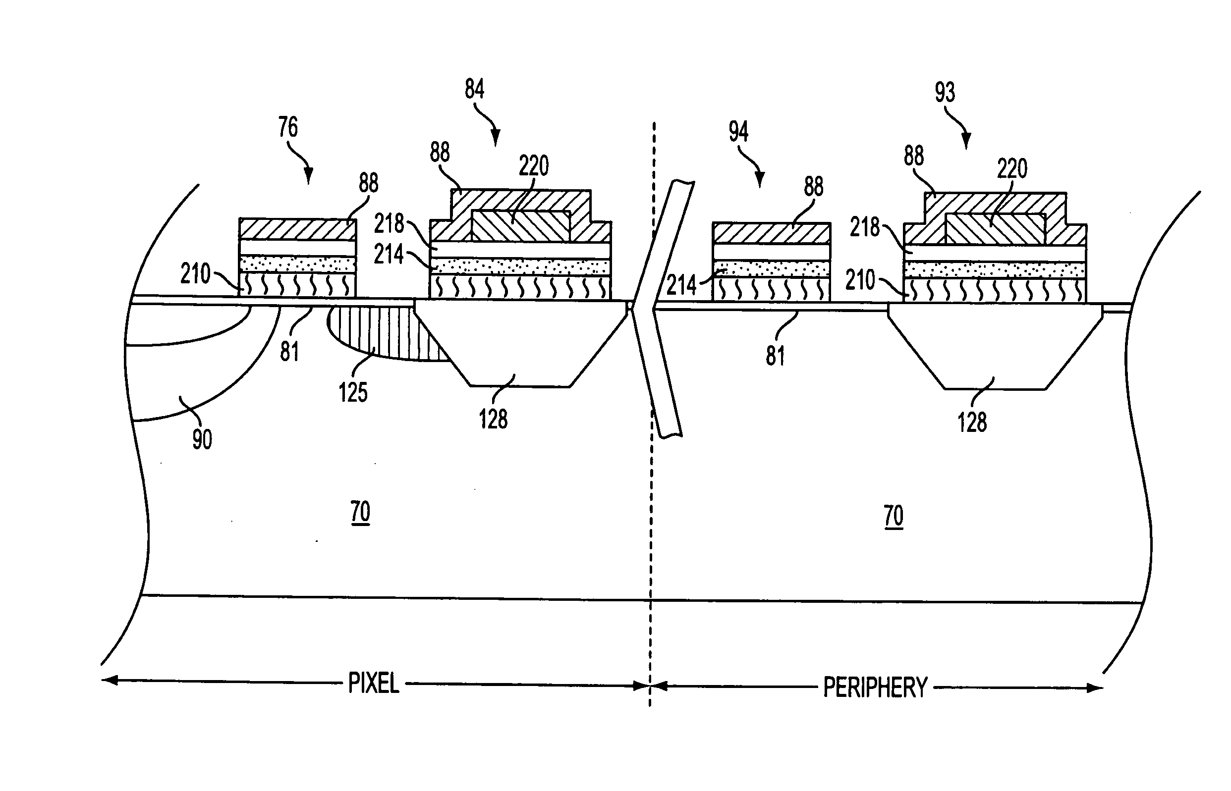
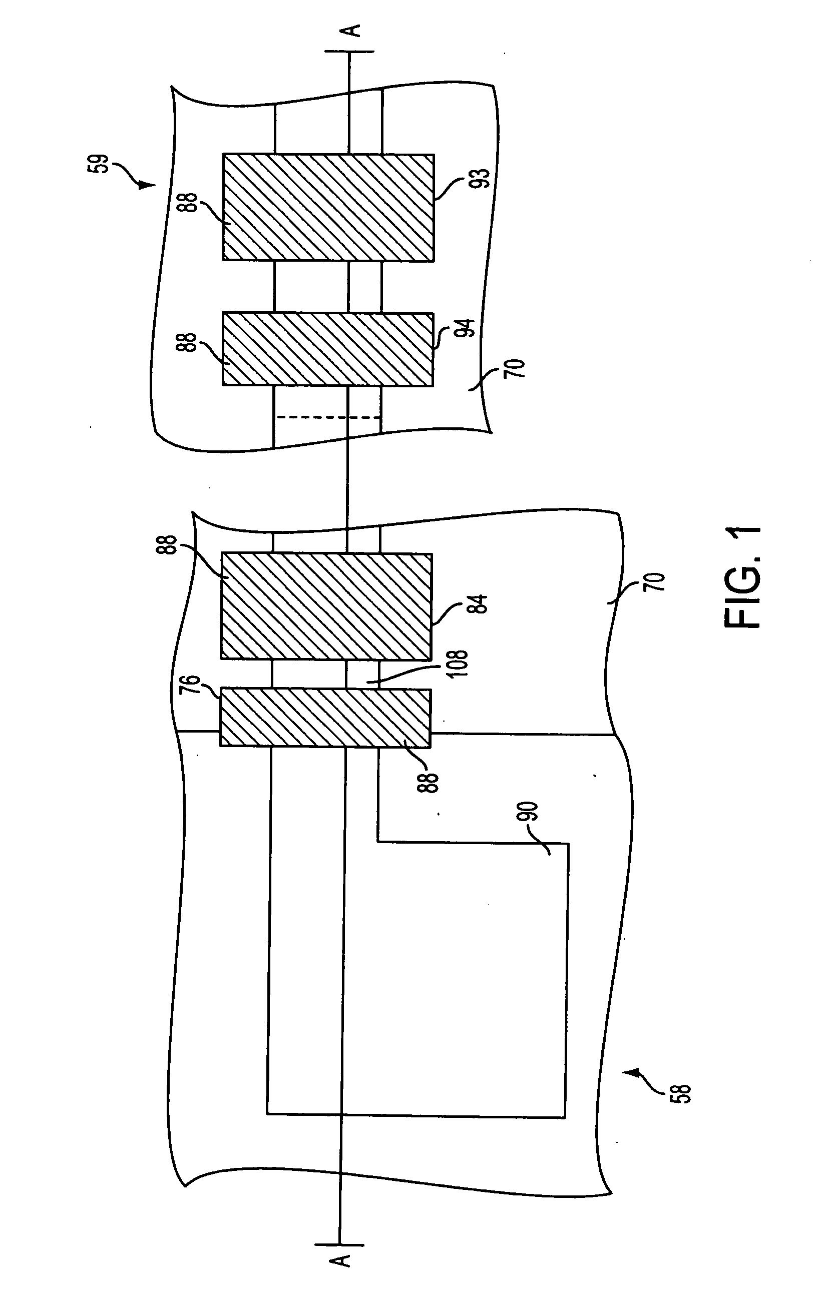
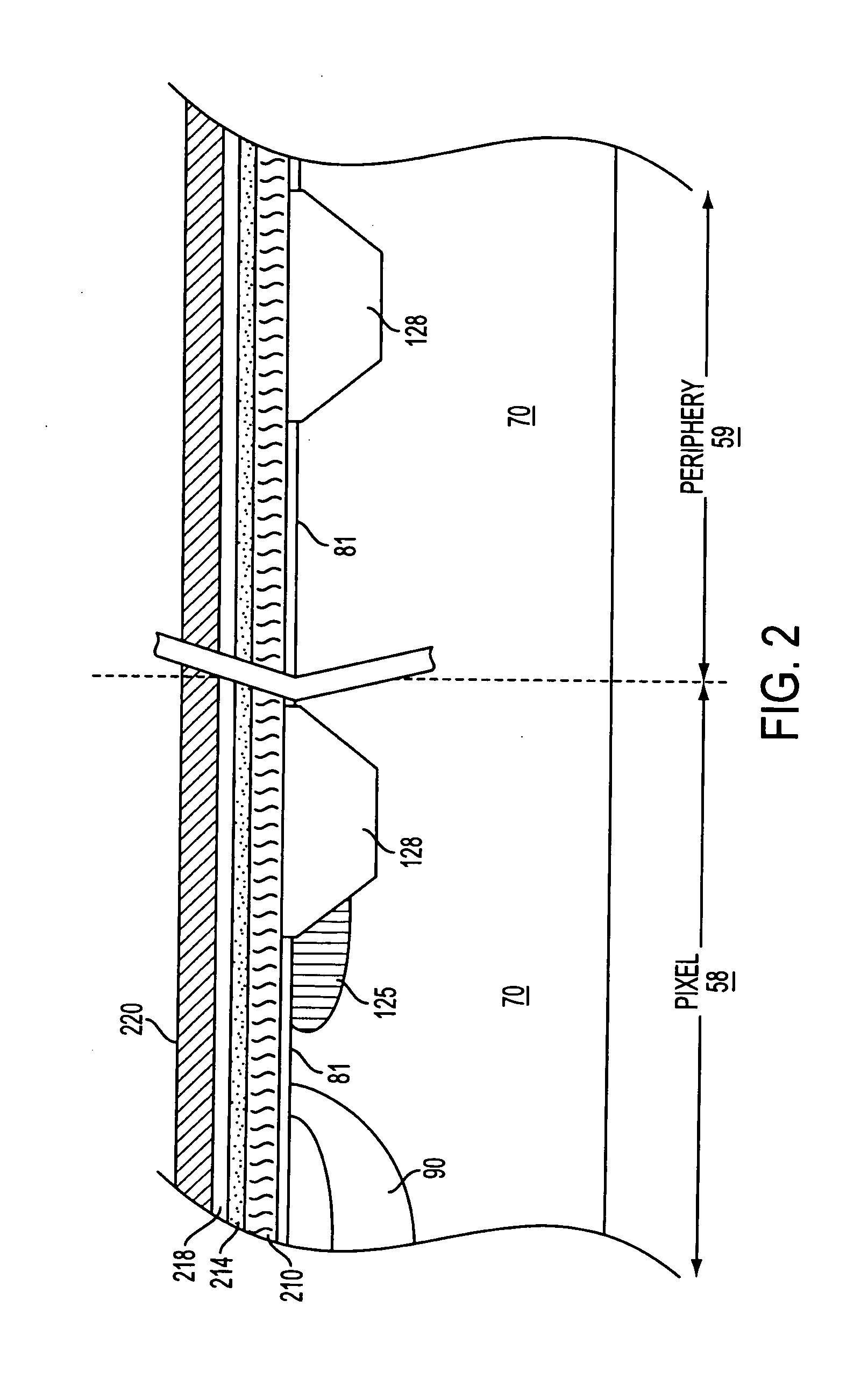
[0027] In the following detailed description, reference is made to various specific embodiments in which the invention may be practiced. These embodiments are described with sufficient detail to enable those skilled in the art to practice the invention, and it is to be understood that other embodiments may be employed, and that structural and logical changes may be made without departing from the spirit or scope of the present invention.

[0028] The terms “substrate” and “wafer” can be used interchangeably in the following description and may include any semiconductor-based structure. The structure should be understood to include silicon, silicon-on insulator (SOI), silicon-on-sapphire (SOS), doped and undoped semiconductors, epitaxial layers of silicon supported by a base semiconductor foundation, and other semiconductor structures. The semiconductor need not be silicon-based. The semiconductor could be silicon-germanium, germanium, or gallium arsenide. When reference is made to the...


PUM


Abstract

CMOS and CCD imaging devices comprising different in-pixel capacitors and peripheral capacitors and methods of formation are disclosed. The capacitors used in periphery circuits have different requirements from the capacitors used in the pixel itself. Dual stack capacitors comprising two dielectric layers may be provided to achieve low leakage and high capacitance. A single masking step may be provided such that one region has a dual dielectric capacitor and a second region has a single dielectric capacitor. A different dielectric may also be provided in one region compared to another region wherein the inter-electrode insulator comprises a single dielectric in both regions.

Description

FIELD OF THE INVENTION [0001] The invention relates to capacitor structures for solid state imaging devices, including CMOS and CCD imaging devices. BACKGROUND OF THE INVENTION [0002] There are a number of different types of semiconductor-based imagers, including charge coupled devices (CCDs), photo diode arrays, charge injection devices and hybrid focal plane arrays. CCDs are often employed for image acquisition for small size imaging applications. However, CCD imagers suffer from a number of disadvantages. For example, they are susceptible to radiation damage, they exhibit destructive read out over time, they require good light shielding to avoid image smear and they have a high power dissipation for large arrays. [0003] Because of the inherent limitations in CCD technology, there is an interest in CMOS imagers for possible use as low cost imaging devices. CMOS imagers have a number of advantages, including for example low voltage operation and low power consumption. CMOS imagers ...

Claims


Application Information

Patent Timeline
IPC IPC(8): H01L27/146
CPCH01L27/14603H01L27/14609H01L27/14689H01L27/14645H01L27/14685H01L27/14643H01L27/146
Inventor RHODES, HOWARD E.
Owner APTINA IMAGING CORP
Why Eureka
Try Eureka