Method and apparatus for a variable processing period in an integrated circuit

a technology of integrated circuits and processing periods, applied in the field of methods and apparatus for a variable processing period in an integrated circuit, can solve the problems of increasing the difficulty of extracting values from algorithms, increasing power consumption, etc., and achieves the effect of increasing power consumption and making current analysis more difficul

Active Publication Date: 2005-04-28
ATMEL CORP
View PDF14 Cites 9 Cited by
  • Summary
  • Abstract
  • Description
  • Claims
  • Application Information

AI Technical Summary

Benefits of technology

[0019] The invention consists of altering, randomly or pseudo-randomly, the number of clock cycles over which an algorithm is performed. The invention may be used in any circuit where digital logic modules are embodied. The invention takes place in the digital part of an integrated circuit. When data is processed in a digital module, combinatorial logic operates and causes an increase in power consumption. The increase in current is primarily due to cell switching, considering only the digital logic. The total cell leakage current is low compared to this switching current.
[0020] The system and method reshapes current consumption in order to make current analysis more difficult. Current reshaping is performed during processing time period by an additional combinatorial circuit. For example, rather than completing a DES algorithm in 16 clock cycles, over each processing time period, the invention completes the DES algorithm over 16 or fewer clock cycles. This increases the difficulty of extracting values from the algorithm because each processing period may have a different number of clock cycles during which the algorithm was performed. Step 2 of 16, for example, will be at two different positions on two different waveforms and superimposing the waveforms will not yield as much useful information as in FIG. 3.

Problems solved by technology

When data is processed in a digital module, combinatorial logic operates and causes an increase in power consumption.
This increases the difficulty of extracting values from the algorithm because each processing period may have a different number of clock cycles during which the algorithm was performed.

Method used


Image

  • Method and apparatus for a variable processing period in an integrated circuit
  • Method and apparatus for a variable processing period in an integrated circuit
  • Method and apparatus for a variable processing period in an integrated circuit

Examples


Embodiment Construction

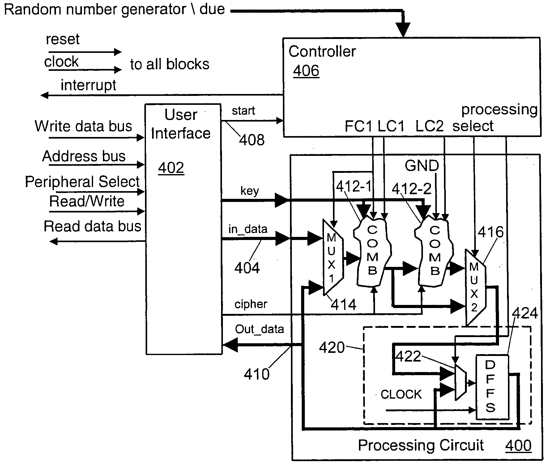
[0031]FIG. 4 is a schematic illustrating one embodiment of the invention in a digital logic module, or a peripheral of a microcontroller. Processing circuit 400 receives input from user interface 402 along input line 404. Controller 406 receives a start signal along start line 408 from user interface 402. Controller 406 transmits a first-cycle signal to processing circuit 400, which begins a processing time period. During a processing time period, processing circuit 400 is manipulating the input in order to produce a desired output, for example an encrypted or decrypted version of the input. Due to the manipulation, for example logic cell switching, processing circuit 400 draws an active range of current during the processing time period and a corresponding waveform of the current over the period may be mapped.

[0032] Processing is typically sixteen clock cycles for a DES algorithm. The invention is a method and system of varying the actual number of clock cycles over which the data...


PUM


Abstract

The invention is a system for modifying the processing period in a digital logic module. The invention comprises the following. A processing circuit is configured to receive an input in order to create an output. A controller is coupled to the processing circuit and is configured to track L manipulations, wherein L is an integer. The controller is further configured to send a select signal to the processing circuit and to cause the processing circuit to manipulate the input over N clock cycles. N is an integer and N is less than or equal to L. N varies over the plurality of processing time periods. An output port is coupled to the processing circuit and is configured to convey the output.

Description

CROSS-REFERENCE TO RELATED APPLICATIONS [0001] This application claims priority to French Application Serial Number 03 12485, filed Oct. 24, 2003. BACKGROUND [0002] 1. Field of the Invention [0003] The invention relates to modifying the processing period in digital logic modules and more particularly to reducing the processing period during encryption / decryption in order to make current analysis more difficult. [0004] 2. Prior Art [0005]FIG. 1 is schematic illustrating a prior art simplified microcontroller. A microcontroller generally includes a microprocessor, memory, a peripheral module that provides communication, for example Universal Asynchronous Receiver / Transmitter (UART), SPI, and USB, and an interrupt controller. Microcontroller 100 includes microprocessor 102 coupled to memory 104. Address decoder 106 receives and decodes addresses from microprocessor 102 for memory 104 and peripherals 108. Address decoder 106 and peripherals 108 receive addresses on address bus 110 while...

Claims


Application Information

Patent Timeline
Patent Type & Authority Applications(United States)
IPC IPC(8): G06F1/32G06F9/302G06F9/318G06F9/38G06F13/10G06F21/55G06J1/00H04L9/06H04L9/18
CPCG06F9/3001G06F9/30181G06F9/3885H04L2209/12H04L9/003H04L9/0625G06F21/558G06F21/755
Inventor VERGNES, ALAIN
Owner ATMEL CORP
Why Eureka
Try Eureka