Byte-wide optical backplane switch and switching method

a backplane switch and optical backplane technology, applied in data switching networks, multiplex communication, instruments, etc., can solve the problems of significant design challenges, difficult to maintain system integrity along the bus, external noise coupled into the interfaces of other components of the system, etc., and achieve the effect of enhancing bandwidth

Inactive Publication Date: 2005-05-05
IBM CORP
View PDF18 Cites 16 Cited by
  • Summary
  • Abstract
  • Description
  • Claims
  • Application Information

AI Technical Summary

Benefits of technology

[0005] Fiber optic communication systems offer significantly enhanced bandwidth compared with copper inter

Problems solved by technology

Radiated electromagnetic noise from copper STI interfaces and external noise coupled into the interfaces from other components in the system pose significant design challenges.
As data rates increase and bus lines become longer, these problems become more significant making it difficult to maintain system i

Method used


Image

  • Byte-wide optical backplane switch and switching method
  • Byte-wide optical backplane switch and switching method
  • Byte-wide optical backplane switch and switching method

Examples


Embodiment Construction

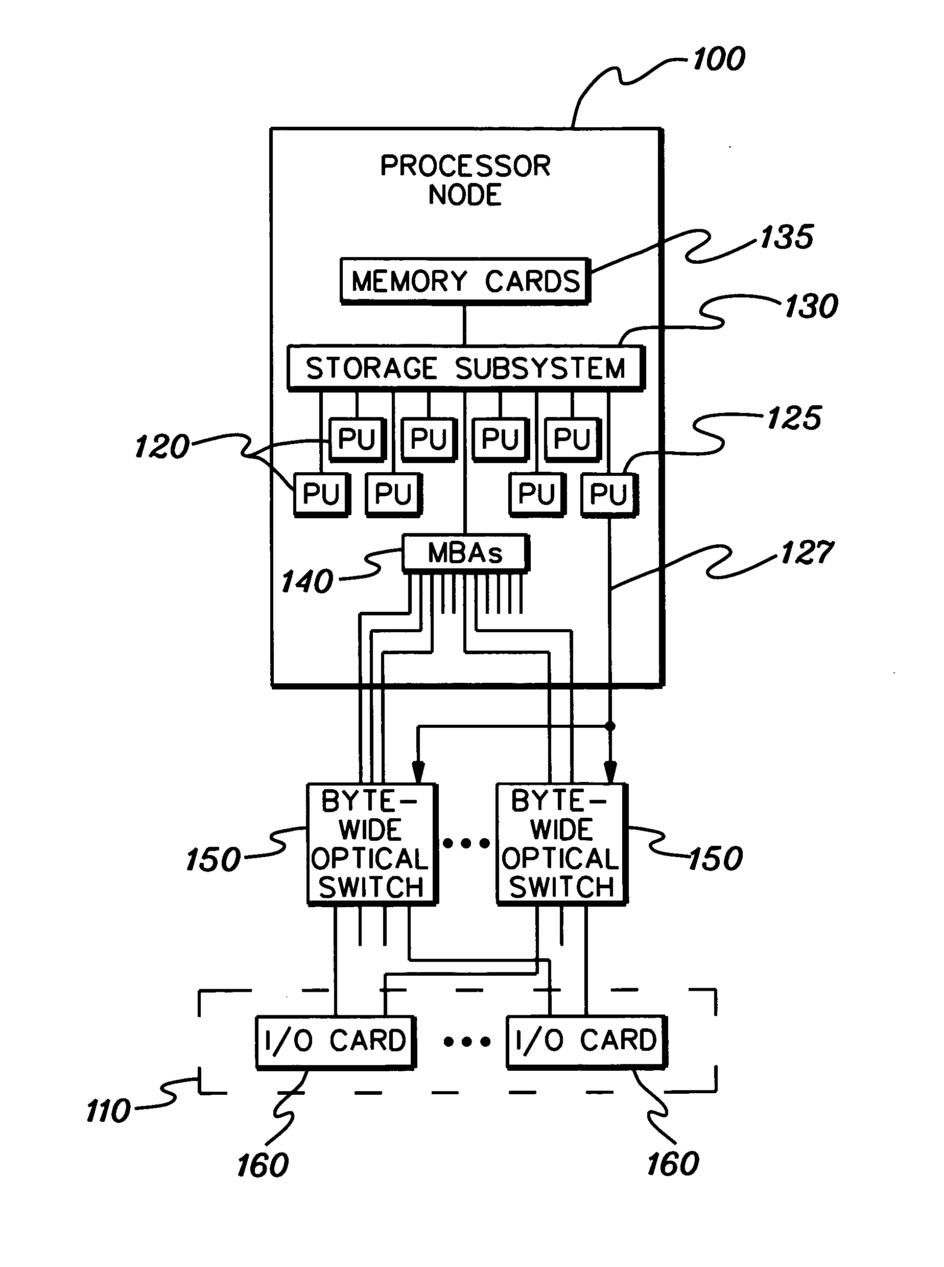
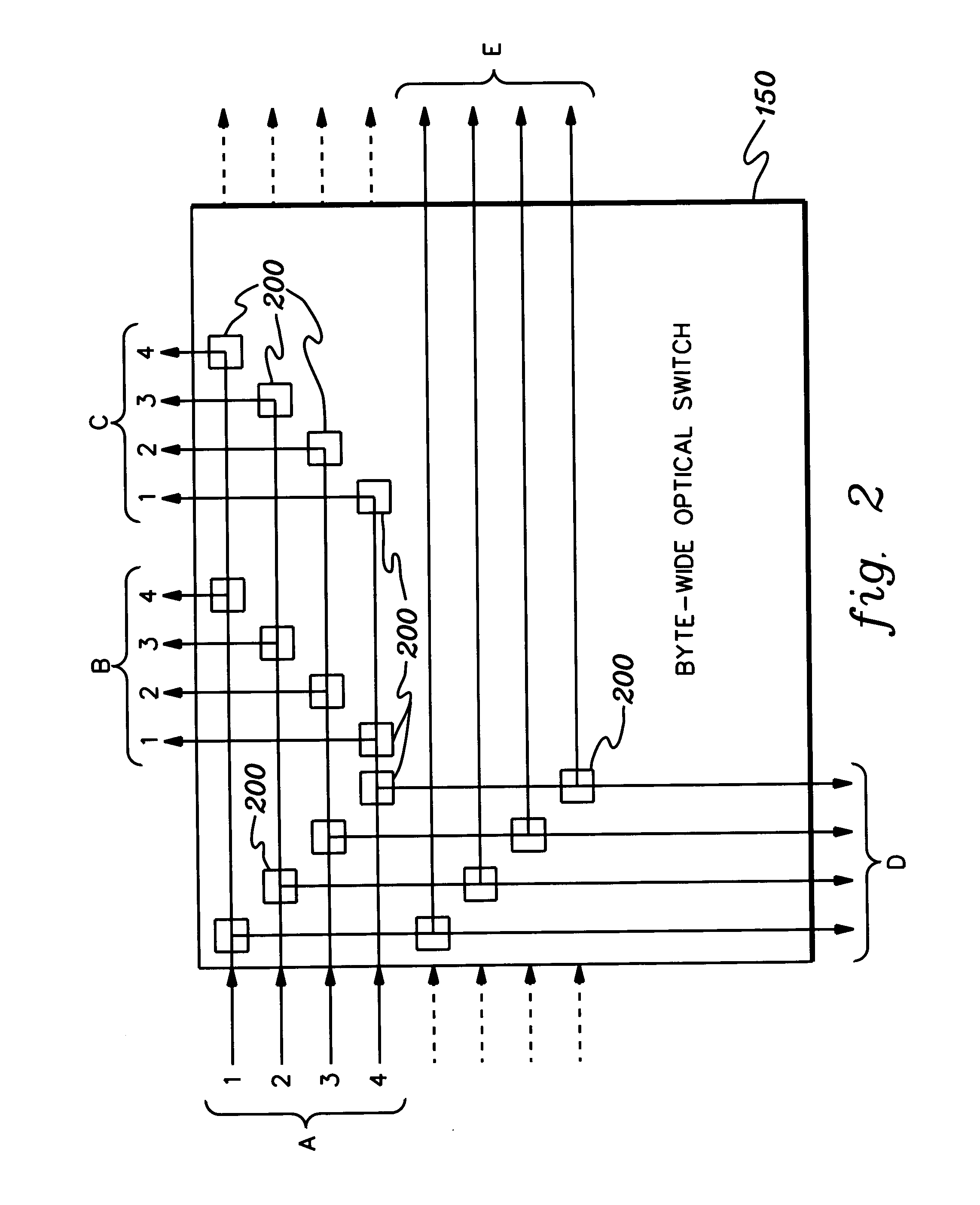
[0019] In U.S. Pat. Nos. 5,333,225, 5,337,388, 5,396,573, and 5,842,881, each of which is hereby incorporated herein by reference in its entirety, interfacing of optical fiber to various types of multichip module packages and multi-layer printed circuit boards is described. Objects of these patents include addressing packaging and mechanical problems involved in combining optical fiber with conventional chip packaging, and bonding techniques. As the applications for optics in the backplane become more mature, there is identified herein a need for optical backplane switching and routing of backplane interconnects. It is not sufficient to simply provide fiber optic I / O to a chip carrier, rather the optical signals must be switched from one location to another, in a manner that provides low latency, high speed, and low jitter and skew, across multiple bit intervals. To achieve low latency and hence better system performance, it is desirable to eliminate the need for serial-to-parallel ...


PUM


Abstract

A byte-wide optical switch and switching method are provided. The optical switch includes a first set of ports for receiving in parallel an optical byte of data, and multiple second sets of ports each capable of outputting in parallel the optical byte of data. An array of optical switching elements is disposed between the first set of ports and the multiple second sets of ports. The array of optical switching elements direct the optical byte of data in parallel from the first set of ports to at least one second set of ports of the multiple second sets of ports. The switching elements may comprise micro-electro mechanical system (MEMS) devices, each having a position controllable reflective surface. Thin film optical filters can be provided on the reflective surfaces for wavelength selective switching.

Description

TECHNICAL FIELD [0001] The present invention relates generally to optical data transfer, and more particularly, to an optical switch for a computing subsystem which receives and switches in parallel an optical byte of data from at least one first set of ports to at least one second set of ports. BACKGROUND OF THE INVENTION [0002] The S / 390 Computing System offered by International Business Machines Corporation currently uses a 12 channel data bus known as a self-timed interface (STI) for many applications within the system architecture. For example, STI is typically used as a connector between a memory bus adapter and an input / output (I / O) subsystem. Radiated electromagnetic noise from copper STI interfaces and external noise coupled into the interfaces from other components in the system pose significant design challenges. As data rates increase and bus lines become longer, these problems become more significant making it difficult to maintain system integrity along the bus. For ex...

Claims


Application Information

Patent Timeline
IPC IPC(8): H04Q11/00
CPCH04Q11/0005H04Q2011/0052H04Q2011/003
Inventor DECUSATIS, CASIMER M.JACOBOWITZ, LAWRENCE
Owner IBM CORP
Why Eureka
Try Eureka