

Nitride semiconductor luminous element and optical device including it
a technology of luminous elements and semiconductors, applied in semiconductor lasers, lasers, solid-state devices, etc., can solve the problems of increase the half-width of emission peak, and difficult to improve the steepness of composition change at the interface, so as to improve the luminous intensity, and reduce the threshold current density
- Summary
- Abstract
- Description
- Claims
- Application Information
AI Technical Summary
Benefits of technology
Problems solved by technology
Method used
Image

Examples
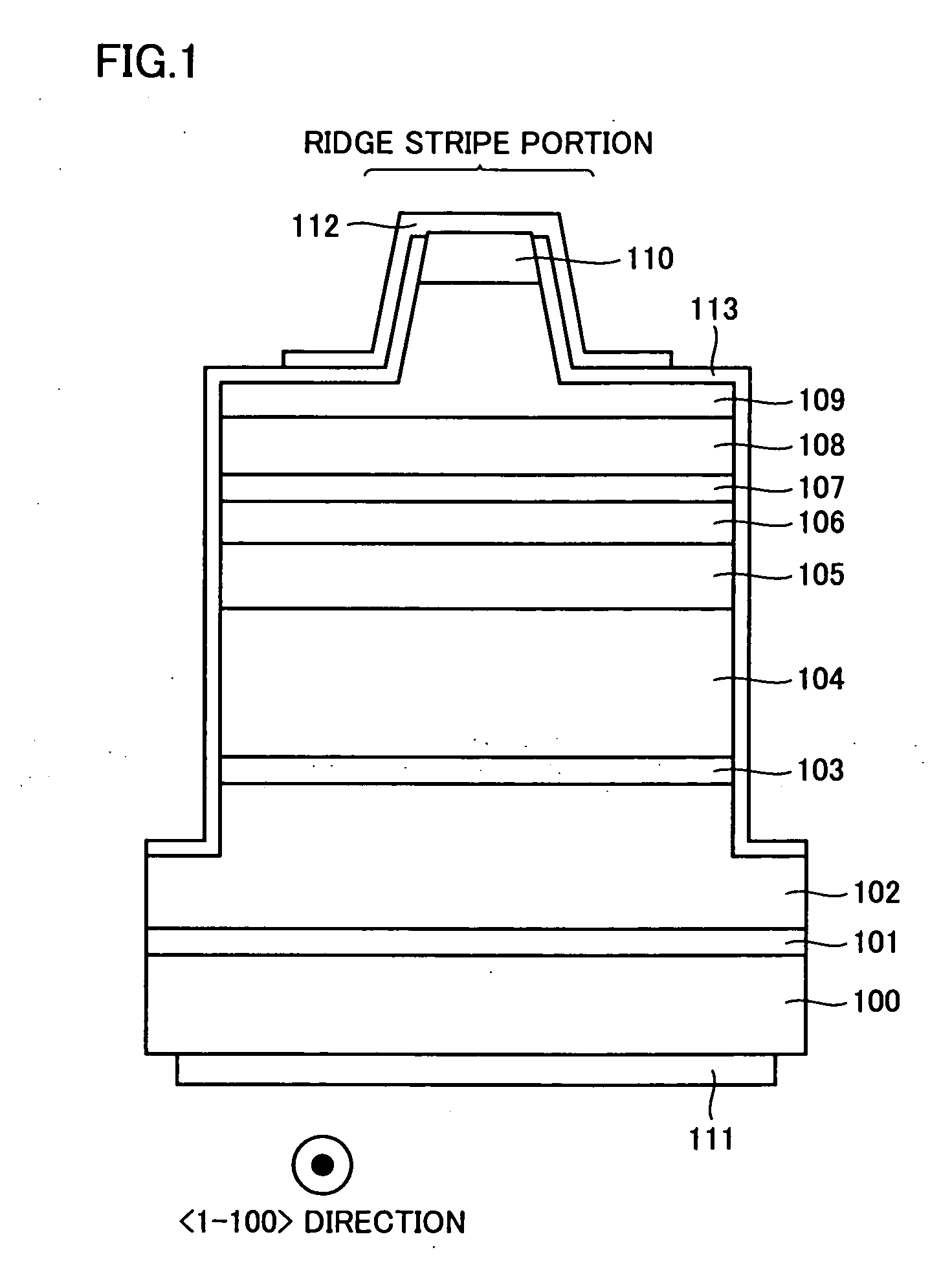
first embodiment
[0042] First Embodiment
[0043] (Light Emitting Layer)
[0044] To solve the problem (of interfacial steepness) of the conventional light emitting layer as described above, in a first embodiment of the present invention, a GaN barrier layer in contact with a GaNX well layer (containing at least one element selected from As, P and Sb as an element X, and having an atomic fraction X / (N+X) of less than 30%) contains a third element Y. At least one element selected from As, P and Sb can be contained as the element Y. Hereinafter, such a barrier layer is referred to as the GaNY barrier layer.
[0045]FIG. 12 shows a result of SIMS carried out in the light emitting layer including GaNAs well layers / GaNAs barrier layers in the present embodiment. In FIG. 12, the well and barrier layers were formed at the same growth temperature (800° C.). As seen from the drawing, interfacial steepness between the well and barrier layers is improved by using the GaNAs barrier layer containing As as the element Y...
second embodiment
[0122] Second Embodiment
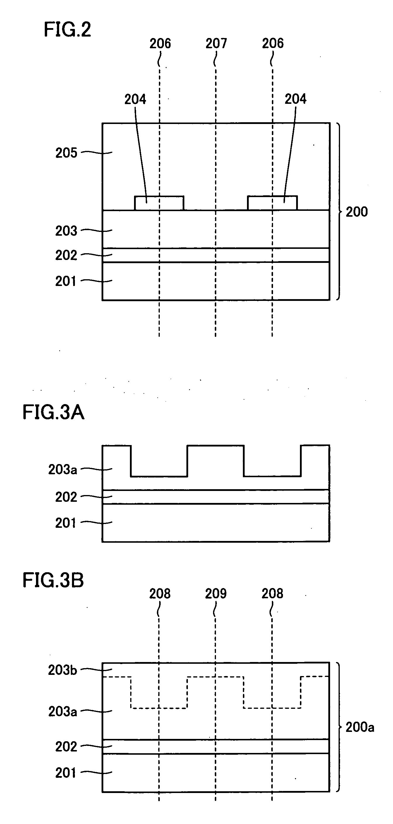
[0123] The second embodiment differs from the first embodiment of FIG. 1 only in that GaN substrate 100 is replaced with a pseudo GaN substrate 200 of FIG. 2 or a pseudo GaN substrate 200a of FIG. 3B, and that the n electrode is formed on the front side of the substrate as shown in FIG. 4.
[0124] The pseudo GaN substrate 200 of FIG. 2 includes a seed substrate 201, a low-temperature buffer layer 202, an n type GaN film 203, a growth inhibiting film 204, and an n type GaN thick film 205. Seed substrate 201 is used as a base material for growing n type GaN thick film 205. The growth inhibiting film refers to a film restricting crystal growth of the nitride semiconductor film thereon. The pseudo GaN substrate described here refers not only to the one having a structure shown in FIG. 2, but also to any other one including at least a seed substrate and a growth inhibiting film.
[0125] The pseudo GaN substrate 200a of FIG. 3B includes a seed substrate 201, a low-te...
third embodiment
[0135] Third Embodiment
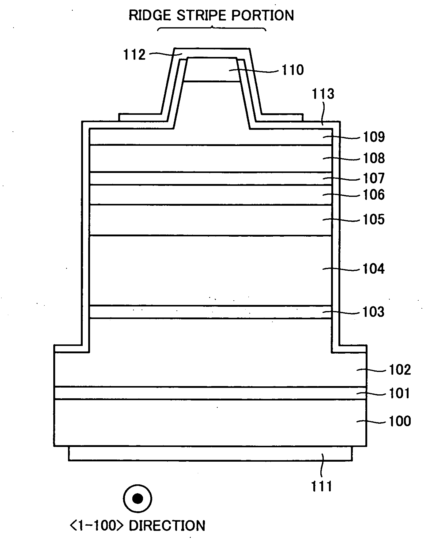
[0136] The third embodiment differs from the embodiment of FIG. 1 only in that the nitride semiconductor laser device is formed on a substrate other than the nitride semiconductor substrate with a nitride semiconductor buffer layer interposed therebetween, and that the n electrode is formed on one side of the substrate as shown in FIG. 4.
[0137] Referring to FIG. 4, the nitride semiconductor laser device of the present embodiment includes a substrate 300, a low-temperature GaN buffer layer 101 (thickness: 25 nm), an n type GaN layer 102, an n type In0.07Ga0.93N anti-crack layer 103, an n type Al0.1Ga0.9N clad layer 104, an n type GaN light guide layer 105, a light emitting layer 106, a p type Al0.2Ga0.8N carrier block layer 107, a p type GaN light guide layer 108, a p type Al0.1Ga0.9N clad layer 109, a p type GaN contact layer 110, an n electrode 111, a p electrode 112, and a SiO2 dielectric film 113. Substrate 300 may be, e.g., a C (0001) plane sapphire subst...
PUM
 Abstract
Description
Claims
Application Information