Solid state photosensitive devices which employ isolated photosynthetic complexes

a photosensitive device and photosensitive technology, applied in the field of solid-state photosensitive devices, can solve the problems of failing to describe a high-efficiency photoconversion structure for trapping and converting incident light into electrical energy suitable for nanometric electronic devices, and exceeding the efficiency of even the best artificial photovoltaic devices

Active Publication Date: 2005-05-12
THE TRUSTEES FOR PRINCETON UNIV
View PDF8 Cites 134 Cited by
  • Summary
  • Abstract
  • Description
  • Claims
  • Application Information

AI Technical Summary

Problems solved by technology

Indeed, natural biomolecular complexes exceed the efficiencies of even the best artificial photovoltaic devices.
The prior art, however, has failed to describe a high efficiency photoconversion structure for trapping and converting incident light to electrical energy suitable for nanometric electronic devices.

Method used


Image

  • Solid state photosensitive devices which employ isolated photosynthetic complexes
  • Solid state photosensitive devices which employ isolated photosynthetic complexes
  • Solid state photosensitive devices which employ isolated photosynthetic complexes

Examples


examples

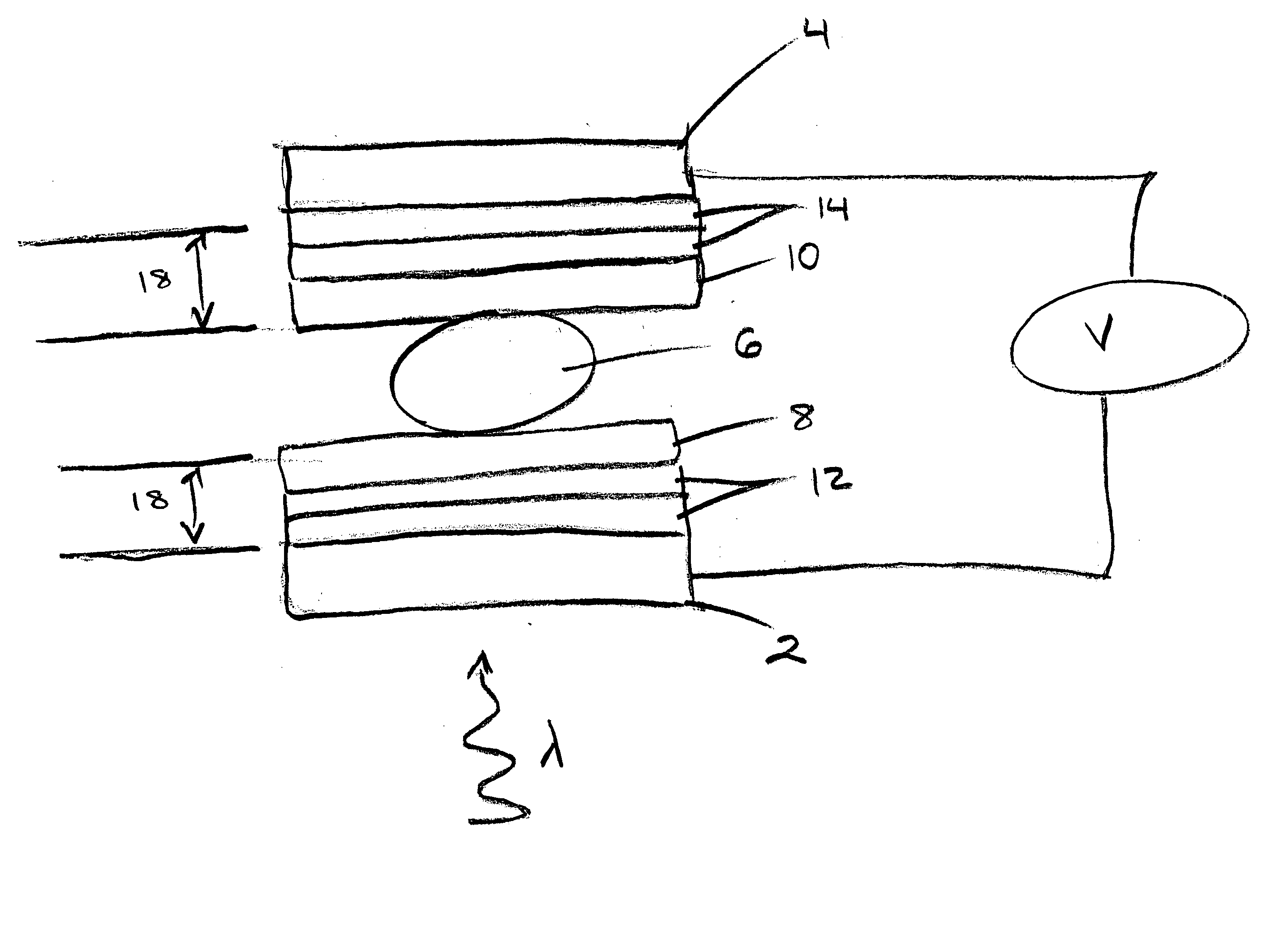
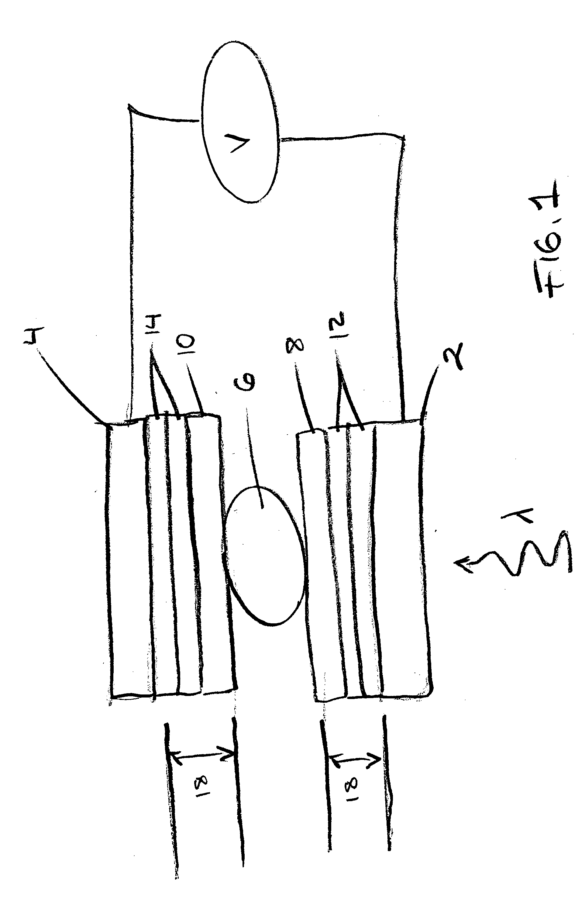
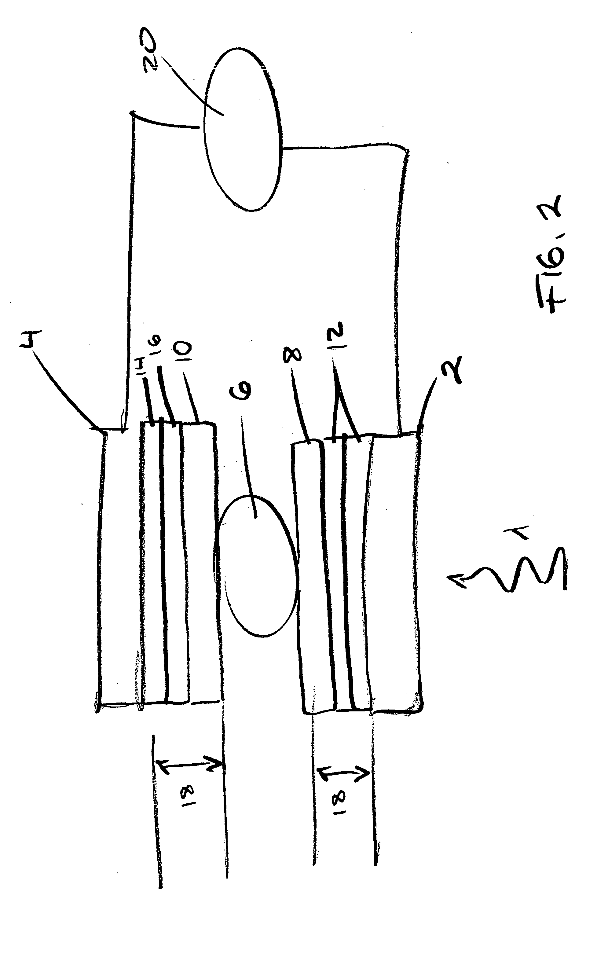
[0052] When depositing metal contacts onto the Light Harvesting Complexes (LHC), care must be taken not to disturb the protein scaffold of the LHC. For this purpose, for example, non-destructive nanometric metal contact stamping techniques are employed. The protein-based complex is interfaced with conventional electronics using a nanopatteming technique. See, e.g., Kim, et al., U.S. Pat. No. 6,468,819, Method For Patterning Organic Thin Film Devices Using A Die; and, Lee, et al., Programmable Nanometer-Scdale Electrolytic Metal Deposition And Depletion, U.S. Pat. No. 6,447,663, each of which is herein incorporated by reference.

example i

[0053] The devices may be constructed (“grown”) from one side. For example, an electrode may first be deposited on a substrate (e.g., glass or plastic). PSI complexes, for example, may be deposited on a transparent indium tin oxide electrode. Metal contacts to the LHC, a PSI complex, for example, may be directly transferred by the ultrahigh resolution, non-damaging stamping process. The formation of metal contacts must be compatible with fragile protein (LHC) complexes. The aim of the technique is the transfer of a metal film at the points of contact between a lithographically patterned stamp and a substrate at resolutions comparable to the diameter of the PSI complexes (about 10 nm). Transfer occurs if the substrate-metal adhesion exceeds adhesion forces between the stamp and the metal layer. To improve transfer, one or more adhesion reduction layers, such as Teflon®, may be deposited between the stamp surface and the metal layer. See FIG. 7 (FIG. 7-9). Prior to step 1, a thin laye...

example ii

[0054] The electrode may be patterned, e.g., lithography. However, patterning may be simultaneously accomplished with the electrode deposition as in I. FIG. 3 shows a schematic diagram of several complexes of LHC sandwiched between silver and transparent indium tin oxide (photovoltaic device). The TIO may be patterned by exposing a self assembled LHC monolayer using electron beam lithography, thereby changing the surface adhesion properties of the LHC complex. The dimensions of the stamped contacts are defined by electron beam lithography. Electron-beam lithography to define raised features on a stamp is well known to people in the art. It involves exposing a resist (polymer, typically PMMA—polymethyl methacrylate) to a fine (˜1 nm) electron beam. Where the resist is exposed, it will dissolve in a weak solvent that leaves the unexposed parts untouched. The resist pattern is then transferred into the stamp material by wet or dry etching techniques.


PUM

PropertyMeasurementUnit
reduction potentialaaaaaaaaaa
semi-transparentaaaaaaaaaa

Abstract

Solid state photosensitive devices including photovoltaic devices are provided which comprise a first electrode and a second electrode in superposed relation; and at least one isolated Light Harvesting Complex (LHC) between the electrodes. Preferred photosensitive devices comprise an electron transport layer formed of a first photoconductive organic semiconductor material, adjacent to the LHC, disposed between the first electrode and the LHC; and a hole transport layer formed of a second photoconductive organic semiconductor material, adjacent to the LHC, disposed between the second electrode and the LHC. Solid state photosensitive devices of the present invention may comprise at least one additional layer of photoconductive organic semiconductor material disposed between the first electrode and the electron transport layer; and at least one additional layer of photoconductive organic semiconductor material, disposed between the second electrode and the hole transport layer. Methods of generating photocurrent are provided which comprise exposing a photovoltaic device of the present invention to light. Electronic devices are provided which comprise a solid state photosensitive device of the present invention.

Description

FIELD OF THE INVENTION [0001] The present invention generally relates to solid state photosensitive devices, including photovoltaic devices, which comprise a first electrode and a second electrode in superposed relation; and at least one isolated photosynthetic complex (Light Harvesting Complex (LHC), e.g., PSI (Photosystem I, from spinach, for example), and / or LH2 (Light Harvesting complex 2, from purple bacteria)) between the electrodes. Methods are described for supplying power to a circuit comprising exposing a photovoltaic device of the present invention to light. Electronic devices are described which incorporate solid state photosensitive devices of the present invention. BACKGROUND OF THE INVENTION [0002] Photosynthesis is the biological process that converts electromagnetic energy into electrochemical energy through light and dark reactions. Photosynthesis occurs in specialized organelles in green algae and higher plants called chloroplasts. The chloroplast is enclosed by a...

Claims


Application Information

Patent Timeline
Patent Type & Authority Applications(United States)
IPC IPC(8): H01L27/30H01L51/00H01L51/30H01L51/40H01L51/42
CPCB82Y10/00H01L27/30H01L51/0004H01L51/0021H01L51/0053Y02E10/549H01L51/0093H01L51/4206H01L51/424H01L51/4246H01L2251/308H01L51/0062H10K39/00H10K71/13H10K71/60H10K85/621H10K85/649H10K85/761H10K30/451H10K30/20H10K30/211H10K2102/103
Inventor PEUMANS, PETERFORREST, STEPHEN R.
Owner THE TRUSTEES FOR PRINCETON UNIV
Why Eureka
Try Eureka