Solid state photosensitive devices which employ isolated photosynthetic complexes
a photosensitive device and photosensitive technology, applied in solid-state devices, organic semiconductor devices, nanometric electronic devices, etc., can solve the problems of failing to describe a high-efficiency photoconversion structure for trapping and converting incident light into electrical energy suitable for nanometric electronic devices
- Summary
- Abstract
- Description
- Claims
- Application Information
AI Technical Summary
Benefits of technology
Problems solved by technology
Method used
Image
Examples
examples
[0054]When depositing metal contacts onto the Light Harvesting Complexes (LHC), care must be taken not to disturb the protein scaffold of the LHC. For this purpose, for example, non-destructive nanometric metal contact stamping techniques are employed. The protein-based complex is interfaced with conventional electronics using a nanopatteming technique. See, e.g., Kim, et al., U.S. Pat. No. 6,468,819, Method For Patterning Organic Thin Film Devices Using A Die; and, Lee, et al., Programmable Nanometer-Scdale Electrolytic Metal Deposition And Depletion, U.S. Pat. No. 6,447,663, each of which is herein incorporated by reference.
example i
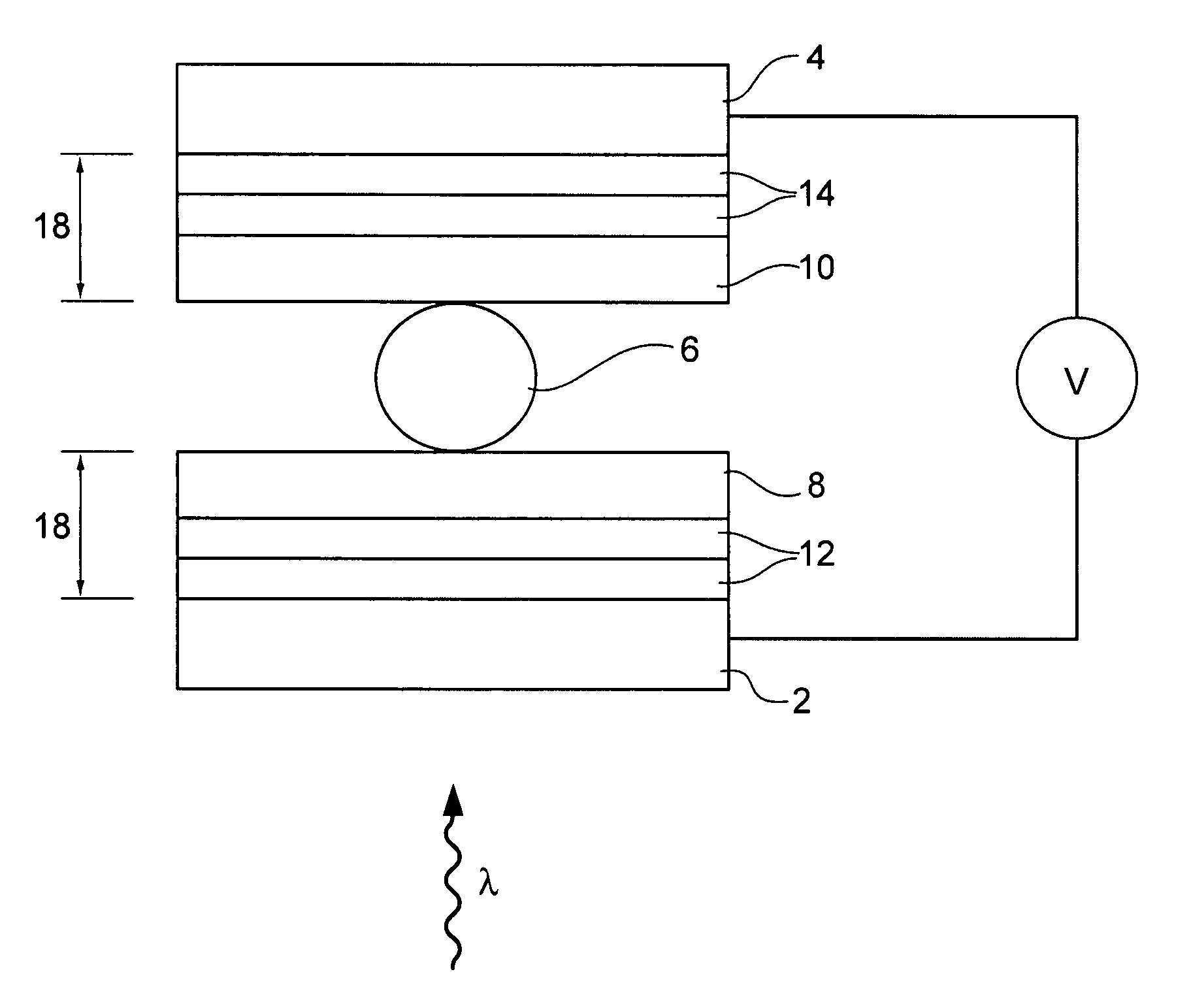
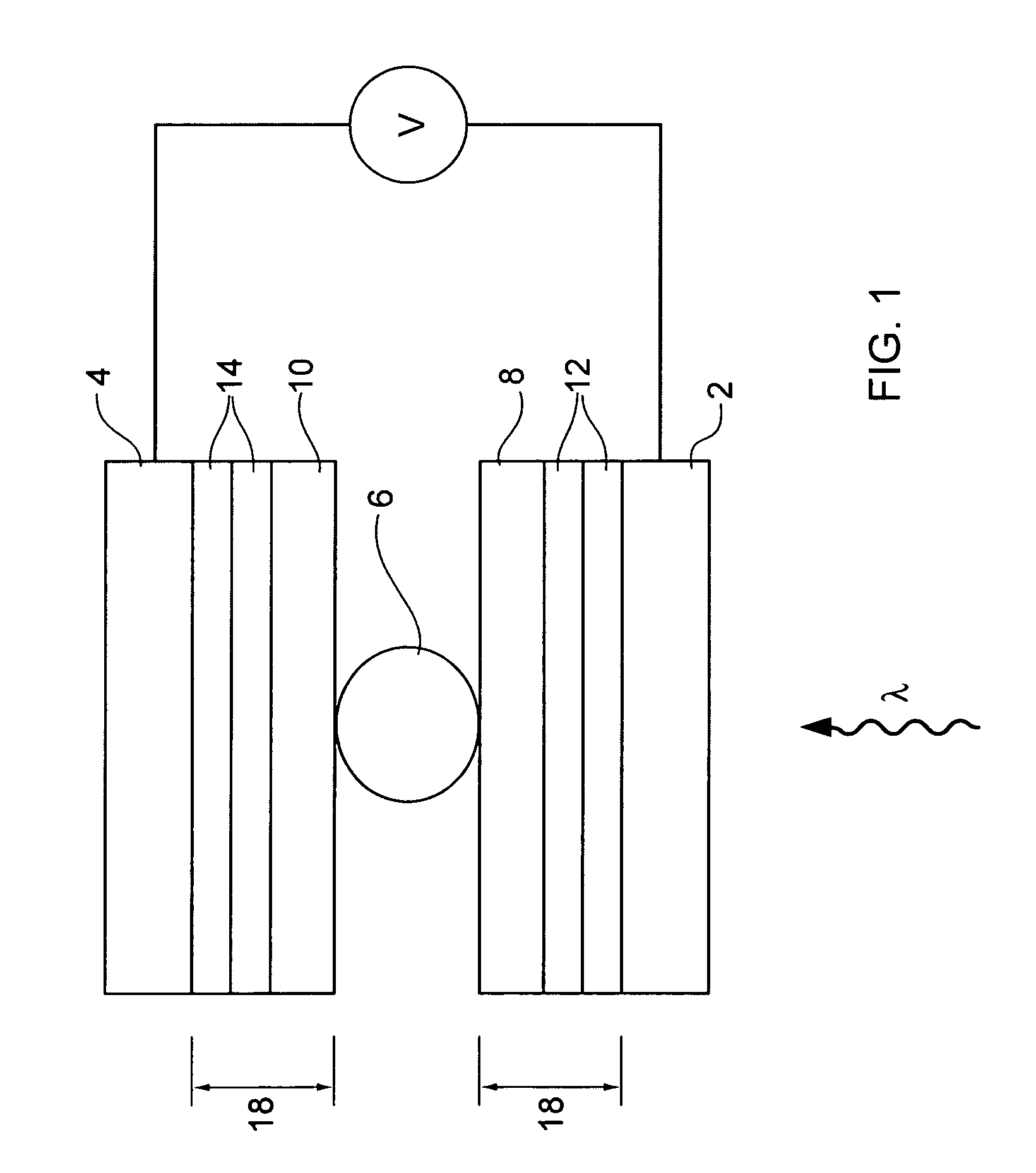
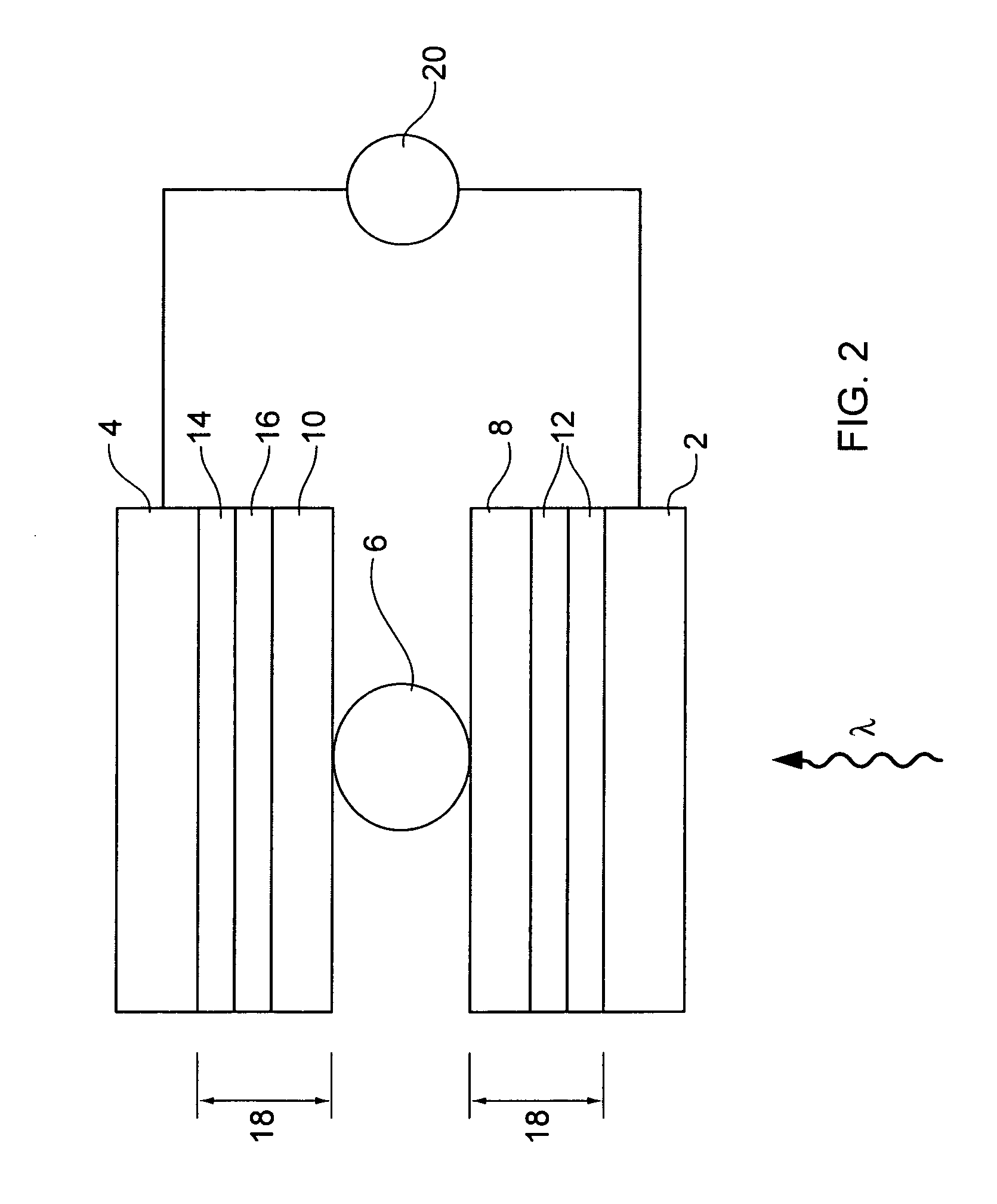
[0055]The devices may be constructed (“grown”) from one side. For example, an electrode may first be deposited on a substrate (e.g., glass or plastic). PSI complexes, for example, may be deposited on a transparent indium tin oxide electrode. Metal contacts to the LHC, a PSI complex, for example, may be directly transferred by the ultrahigh resolution, non-damaging stamping process. The formation of metal contacts must be compatible with fragile protein (LHC) complexes. The aim of the technique is the transfer of a metal film at the points of contact between a lithographically patterned stamp and a substrate at resolutions comparable to the diameter of the PSI complexes (about 10 nm). Transfer occurs if the substrate-metal adhesion exceeds adhesion forces between the stamp and the metal layer. To improve transfer, one or more adhesion reduction layers, such as Teflon®, may be deposited between the stamp surface and the metal layer. See FIG. 7 (FIG. 7-9). Prior to step 1, a thin layer...
example ii
[0056]The electrode may be patterned, e.g., lithography. However, patterning may be simultaneously accomplished with the electrode deposition as in I. FIG. 3 shows a schematic diagram of several complexes of LHC sandwiched between silver and transparent indium tin oxide (photovoltaic device). The TIO may be patterned by exposing a self assembled LHC monolayer using electron beam lithography, thereby changing the surface adhesion properties of the LHC complex. The dimensions of the stamped contacts are defined by electron beam lithography. Electron-beam lithography to define raised features on a stamp is well known to people in the art. It involves exposing a resist (polymer, typically PMMA—polymethyl methacrylate) to a fine (˜1 nm) electron beam. Where the resist is exposed, it will dissolve in a weak solvent that leaves the unexposed parts untouched. The resist pattern is then transferred into the stamp material by wet or dry etching techniques.
PUM
 Abstract
Description
Claims
Application Information


