Light-emitting component and process for its preparation

a light-emitting component and light-emitting diode technology, applied in the field of light-emitting components, can solve the problems of not being able to rationally apply more than two different polymeric layers, affecting the efficiency of light-emitting diodes, etc., to achieve the effect of easy structurability and greater flexibility in the layer composi

Active Publication Date: 2005-05-26
NOVALED GMBH
View PDF5 Cites 95 Cited by
  • Summary
  • Abstract
  • Description
  • Claims
  • Application Information

AI Technical Summary

Benefits of technology

[0030] This object is achieved from the arrangement point of view by arranging at least one polymer layer and two molecular layers, and, when the cover contact is a cathode, the layer adjacent to the cover contact is formed as an electron-transporting molecular layer and is doped with an organic or inorganic dopant, the n-type dopant containing a principal organic substance and a donor-type doping substance, and the molecular weight of the dopant is greater than 200 g/mole; or, when the cover contact is an anode, the layer adjacent t

Problems solved by technology

The drawback consists, among other things, in the fact that not more than two different polymeric layers can be rationally applied, since the solvents of the polymers must be selected in such a way that they do not mutually affect each other, and, in other words, they do not attack the substrate material.
This means that the emitting polymer must also be simultaneously well suited for both electron transport and electron injection from the cathode, a requirement which represents a serious limitation in the selection of material and structure optimization.
This is disadvantageous particularly for the integration of the PLEDs on active-matrix display substrates with n-channel transistors as a switch component.
The use of transparent cover contacts (also as cathode) is just as difficult, since they are usually prepared by a sputter process (e.g., ITO).
However, this destroys organic materials.
However, even in this case the electron injection from the cathode represents a problem.
A further drawback of the above structure is that an efficient electron injection can be achieved only with very unstable contact materials such as barium or calcium.
These materials, however, are attacked by oxygen and water.
Advantages of this structure are the separate optimizability of the properties of the individual layers, the large adjustable distance between the emitter layer and the contacts, the

Method used


Image

  • Light-emitting component and process for its preparation
  • Light-emitting component and process for its preparation
  • Light-emitting component and process for its preparation

Examples


Embodiment Construction

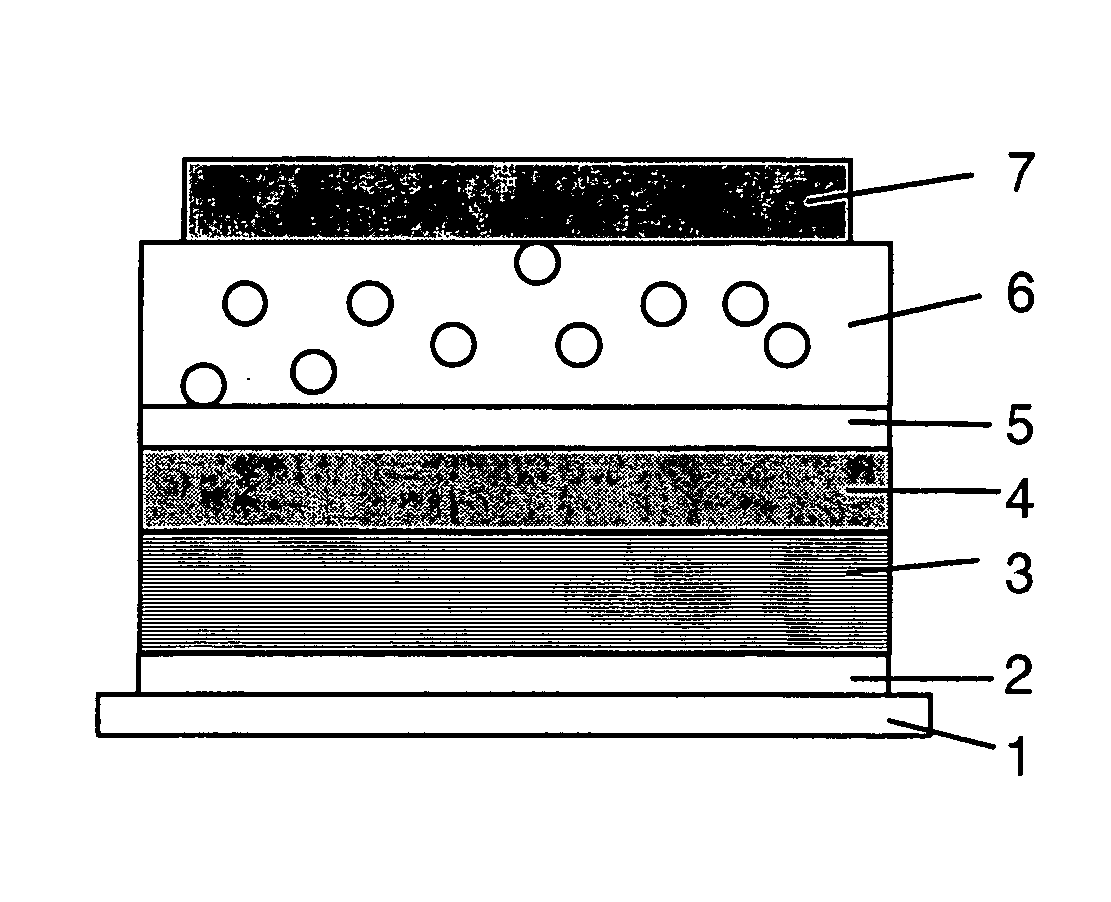
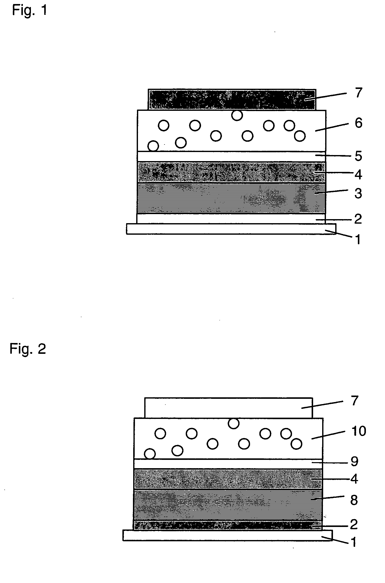
[0042] As shown in FIG. 1, a transparent base contact 2 is placed as anode on a substrate 1. Deposited on this base contact 2 is a first polymer layer as polymeric hole-transporting layer 3, and a second polymer layer as polymeric emitter layer 4. This layer composite of a first and second polymer layer consists of PEDIT:PSS (Baytron-P) of H. C. Stark, Germany. Vapor deposited thereon is a first molecular layer as intermediate layer 5 which consists of a 10 nm layer of BPhen (batophenanthroline). Arranged thereon is a second molecular layer in the form of an electron-transporting layer and injecting layer 6 of BPhen:Cs (molar doping concentration about 10:1 to 1:1). Finally, the organic light-emitting diode according to FIG. 1 is provided with an aluminum cover contact 7.

[0043] In this connection, Cs can be regarded as a non-expedient electron-yielding dopant, since the molecular weight of Cs is too low to be able to achieve a diffusion-stable doped layer therewith. Provided, there...


PUM

PropertyMeasurementUnit
Thicknessaaaaaaaaaa
Thicknessaaaaaaaaaa
Thicknessaaaaaaaaaa

Abstract

A light-emitting component comprising organic layers and having several layers between a base contact and a cover contact, the corresponding process for its preparation. At least one polymer layer and two molecular layers are arranged, so that when the cover contact is a cathode, the layer adjacent to the cover contact is designed as an electron-transporting molecular layer and is doped with an organic or inorganic donor, the electron-transporting layer comprising a principal organic substance and a donor-type doping substance, the molecular weight of the dopant being more than 200 g/mole. When the cover contact is an anode, the layer adjacent to the cover contact is designed as a p-doped hole-transporting molecular layer and is doped with an organic or inorganic acceptor, the hole-transporting layer comprising a principal organic substance and an acceptor-like doping substance, the molecular weight of the dopant being more than 200 g/mole.

Description

CROSS-REFERENCE TO RELATED APPLICATION [0001] The present application claims priority from German Patent Application No. 103 39 772.8-3, filed Aug. 27, 2003, the entire disclosure of which incorporated herein by reference. FIELD OF THE INVENTION [0002] The present invention relates to a light-emitting component comprising organic layers, and in particular to an organic light-emitting diode, consisting of several layers between a base contact on a substrate and a cover contact. The present invention also relates to a processes for the preparation of a light-emitting component, in which a base contact, several layers, and a cover contact are arranged on a substrate. BACKGROUND OF THE INVENTION [0003] Ever since the demonstration of low operating voltages by Tang et al. 1987 (C. W. Tang et al., Appl. Phys. Lett. 51(12), 913 (1987)), organic light-emitting diodes have been promising candidates for the realization of large-area displays and other uses, such as, e.g., lighting elements. T...

Claims


Application Information

Patent Timeline
IPC IPC(8): H01L33/00C09K11/06H01L51/00H01L51/30H01L51/40H01L51/50H05B33/10H05B33/14
CPCH01L51/002H01L51/0037H01L51/0051H01L51/5052H01L51/0077H01L51/5048H01L51/0059H10K71/30H10K85/1135H10K85/611H10K85/631H10K85/30H10K50/14H10K50/155H10K50/165H10K50/15H10K50/171H10K50/11
Inventor BLOCHWITZ-NIMOTH, JANSORIN, GILDAS
Owner NOVALED GMBH
Why Eureka
Try Eureka