Chromatic aberration corrector for charged particles and charged-particle optical apparatus using the corrector
a charged particle and optical apparatus technology, applied in the direction of instruments, mass spectrometers, beam deviation/focusing by electric/magnetic means, etc., can solve the problem that the expected aberration correction effect cannot be sufficiently obtained, the aberration correction cannot be realized in reality, and it is difficult to adjust the aberration correction for arbitrary optical conditions. , to achieve the effect of stabilizing chromatic aberration correction, avoiding aberration, and improving chromatic aberration correction accuracy
- Summary
- Abstract
- Description
- Claims
- Application Information
AI Technical Summary
Benefits of technology
Problems solved by technology
Method used
Image
Examples
embodiment 1
[0032] An embodiment will be described below with the drawings.
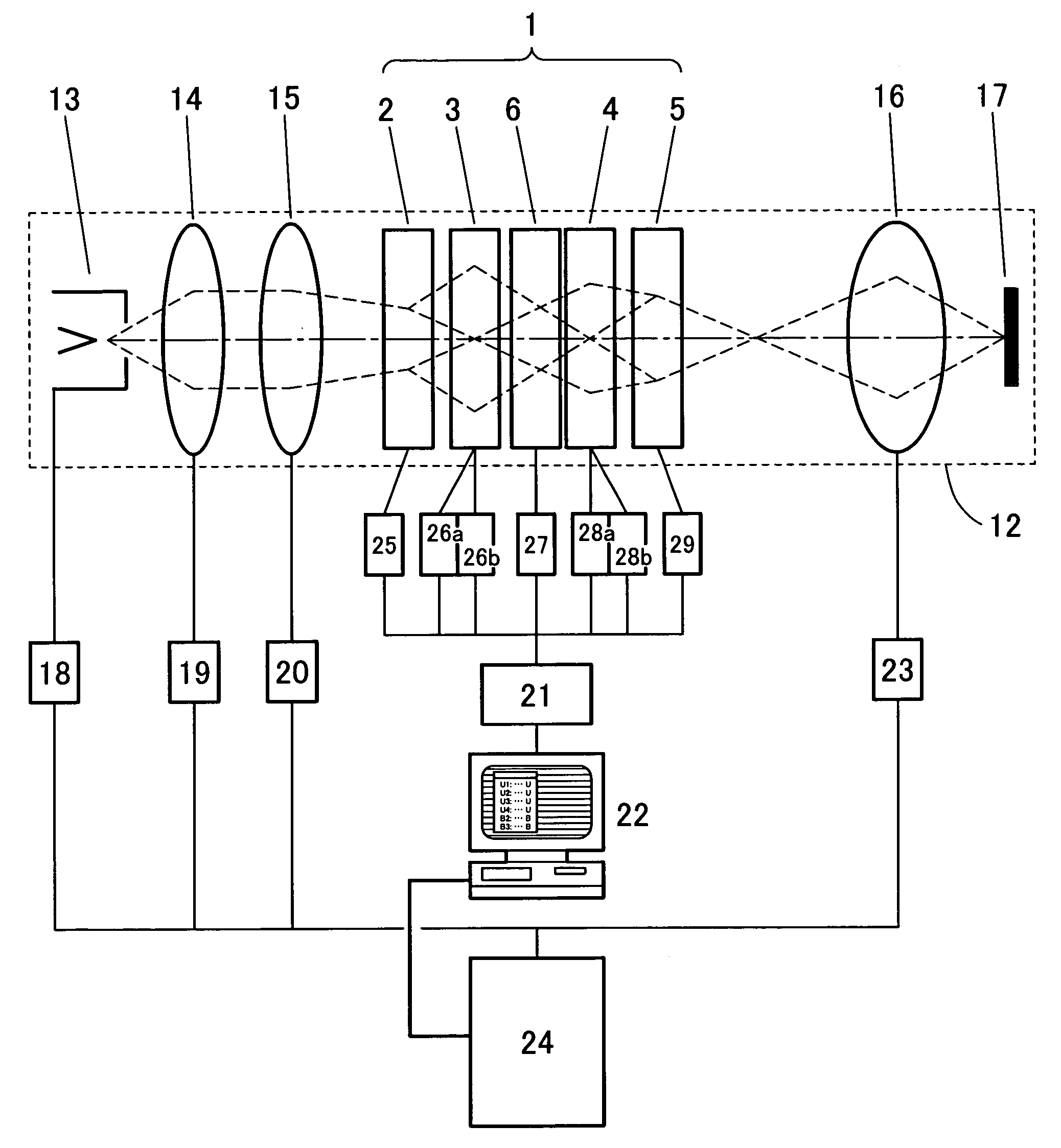
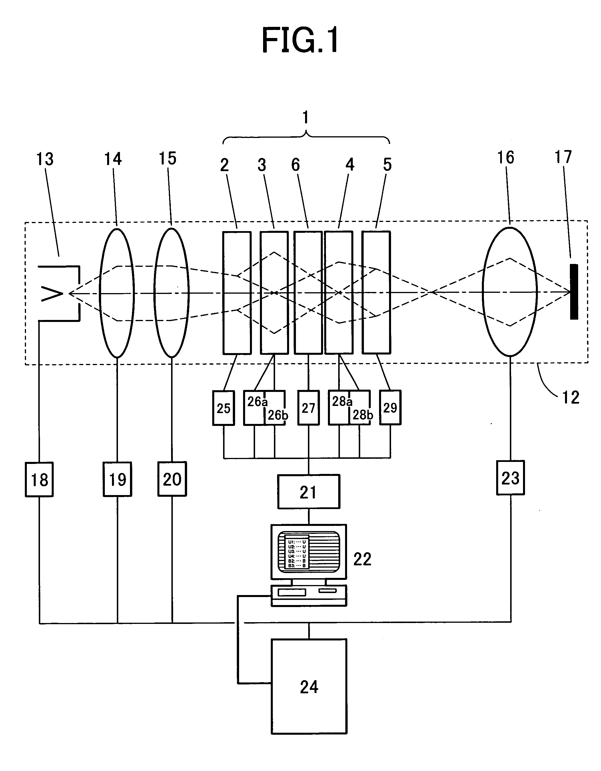
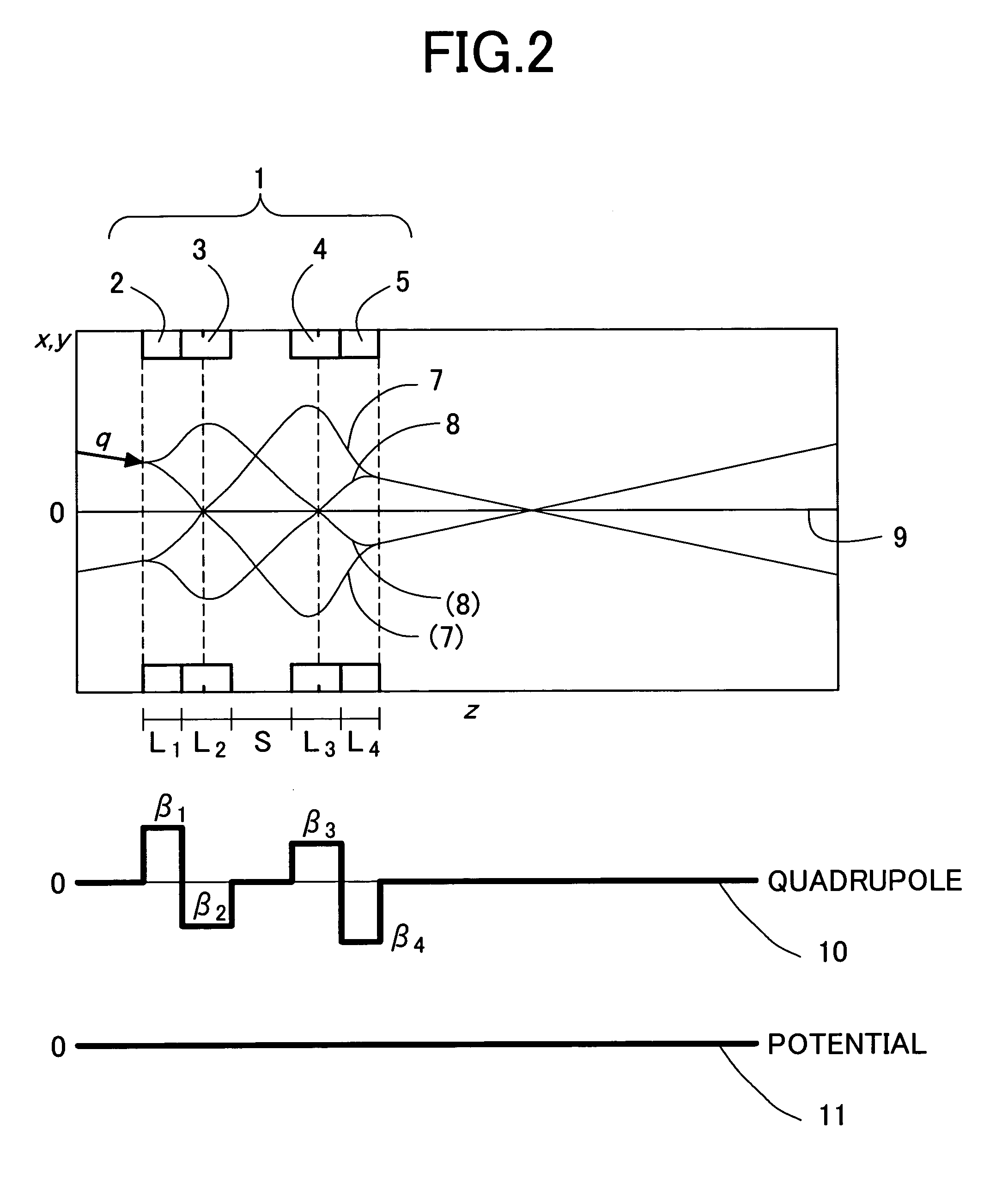
[0033]FIG. 1 shows an embodiment of an SEM. FIG. 1 includes main elements of an electron optics system of the SEM. An electron beam emitted from an electron source 13, after adjustment of the amount of a beam current by condenser lenses 14 and 15, forms a crossover in the position suitable for an objective lens 16. This beam crossover is demagnified and projected onto a sample surface 17 by the objective lens 16 to be a beam probe. The beam probe is scanned on the sample surface by deflector coils, not shown, to produce secondary electrons owing to the electron beam illumination. By measuring the amount of the secondary electrons in positions on the sample surface, “scanning electron microscope image (SEM image)” is thereby obtained. Apparatus and devices which are not important in the description of the present invention, such as a secondary electron detector, a sample stage holding a sample, and aperture apparatus to ...
embodiment 2
[0048]FIG. 5 shows a constructional example different from FIG. 3. The 12 poles 3 and 4 in the second and third stages and the intermediate potential electrodes are used together to apply the intermediate potential Vm added to the potential for multipole field formation. The space between the second and third stages of the multipole lenses becomes an intermediate potential region. In FIG. 5, the voltage sources 26, 28, and 27 are connected in series to superimposed intermediate potentials on multipole potentials.
[0049]FIG. 6 shows results obtained by simulating changes in trajectories in the corrector when the intermediate potential is varied. In the simulation, the incident condition to the corrector is fixed, and rectangle-like distribution of electrical potentials and quadrupole field strengths are assumed. The numerals 7a, 7b and 7c denote an x trajectory and the numerals 8a, 8b and 8c denote a y trajectory. The calculation conditions to a, b and c are summarized in Table 1. A ...
embodiment 3
[0050] In Embodiments 1 and 2, the multipole lenses are assembled in four stages and the intermediate potential region is formed between the inner multipole lenses. However, the intermediate potential region may be formed in a space between other stages or in a plurality of spaces between the stages, not between the multipole lenses arranged in the center.
[0051] In Embodiments 1 and 2, the intermediate potential region 6 is formed only in the space between the stages of the second-stage multipole lens 3 and the third-stage multiple lens 4. In the constructional example shown in FIG. 7, the intermediate potential regions are provided in all three spaces between the stages of the 1-2 (6A), 2-3 (6B), and 3-4 (6C). Such a plurality of intermediate potential regions can be realized by providing the intermediate potential electrode structures 6a, 6b, 6c and 6d of FIG. 3 in the spaces between the stages of the multipole lenses, respectively.
[0052] The intermediate potentials are supplied...
PUM
 Abstract
Description
Claims
Application Information
 - R&D
- Intellectual Property
- Life Sciences
- Materials
- Tech Scout
- Unparalleled Data Quality
- Higher Quality Content
- 60% Fewer Hallucinations
Browse by: Latest US Patents, China's latest patents, Technical Efficacy Thesaurus, Application Domain, Technology Topic, Popular Technical Reports.
© 2025 PatSnap. All rights reserved.Legal|Privacy policy|Modern Slavery Act Transparency Statement|Sitemap|About US| Contact US: help@patsnap.com


