Semiconductor device

a technology of bipolar transistors and semiconductors, applied in the direction of semiconductor devices, basic electric elements, electrical equipment, etc., can solve the problems of increased turn-on resistance, increased turn-on resistance when a large current is flowing, and raised turn-on resistance, rather than being lowered, so as to achieve high power-added efficiency, further lowering turn-on resistance, and high power-added efficiency

Inactive Publication Date: 2005-05-19
RENESAS ELECTRONICS CORP
View PDF3 Cites 16 Cited by
  • Summary
  • Abstract
  • Description
  • Claims
  • Application Information

AI Technical Summary

Benefits of technology

[0018] Next, the action of the P-type δ-doped region and of the P++ GaAs layer is explained. The newly added P-type δ-doped region 12 and P++ GaAs layer 17 can raise the built-in potential with the N-type hole barrier thin film layer 8a. By this means, the electric field felt by the N-type hole barrier thin film layer 8a can be increased, so that the turn-on resistance can be further lowered.
[0019] As explained above, a first advantageous result of this invention is the ability to provide a semiconductor device which, while lowering the offset voltage, lowers the turn-on resistance, to realize a high power-added efficiency. This is because, by placing a hole barrier layer employing semiconductor material with a wide band gap in direct contact with the base layer, the potential barrier arising on the conduction band side of the hole barrier layer can be made a triangular potential barrier, and the turn-on resistance can be lowered.
[0020] A second advantageous result is the ability to provide a semiconductor device in which the base-collector capacitance can be reduced, so that a high power gain is realized. This is because there is no spacer layer between the base layer and hole barrier layer, so that accumulation of carriers occurring between the hole barrier and the spacer layer does not occur.

Problems solved by technology

A material with a wide band gap is used to form the hole barrier; but normally, in addition to the valence band discontinuity, a conduction band discontinuity also occurs, resulting in the problem that the turn-on resistance is increased.
However, there are a number of problems with the HBTs disclosed in the prior art examples 1, 2 and 3.
A first problem is the fact that by introducing the GaAs spacer layer 8d, the turn-on resistance, rather than being lowered, is raised.
A second problem is that the turn-on resistance when a large current is flowing is increased.
A third problem is that the base-collector capacitance is increased.

Method used


Image

  • Semiconductor device
  • Semiconductor device
  • Semiconductor device

Examples


embodiment 1

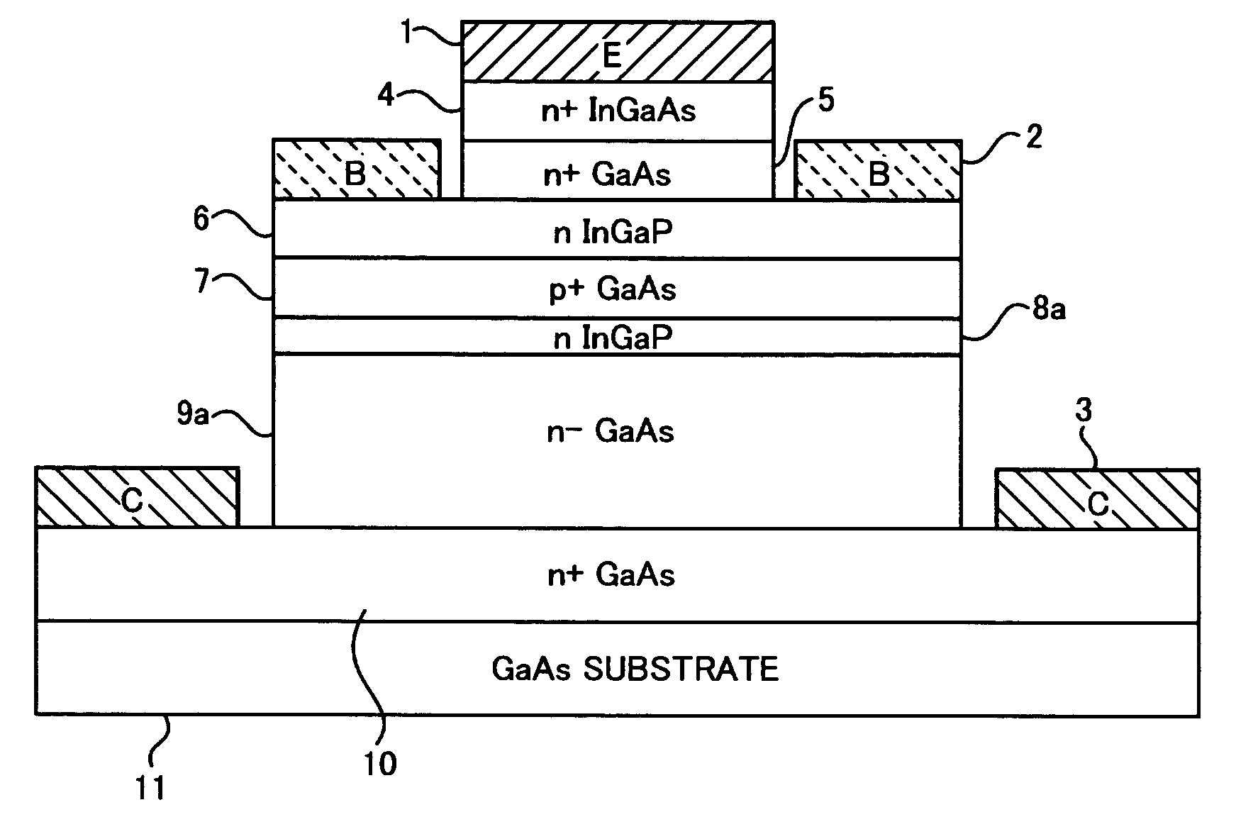
[0048] Embodiment 1, based on the first aspect of this invention, is explained in detail referring to FIG. 1 and to FIG. 14 through FIG. 16 illustrating advantageous results of the invention. FIG. 16 shows current-voltage characteristics in Gm mode. The vertical axis plots the collector current density; the horizontal axis plots the layer thickness of the N-type hole barrier thin film layer 8a in FIG. 1 of this invention. The N-type hole barrier thin film layer 8a used in these measurements had a doping concentration of 2×1018 cm−3, and was an ordering-system In0.48Ga0.52P with a band gap of 1.85 eV. Here “ordering-system” denotes growth under grown conditions such that a natural superlattice is formed in the InGaP layer. An ordering-system has a somewhat lower band gap Eg compared with a disordering-system, but has a smaller conduction band discontinuity. As a result, from the standpoint of reducing the turn-on resistance, it is preferable to use ordering-system InGaP as the N-type...

embodiment 2

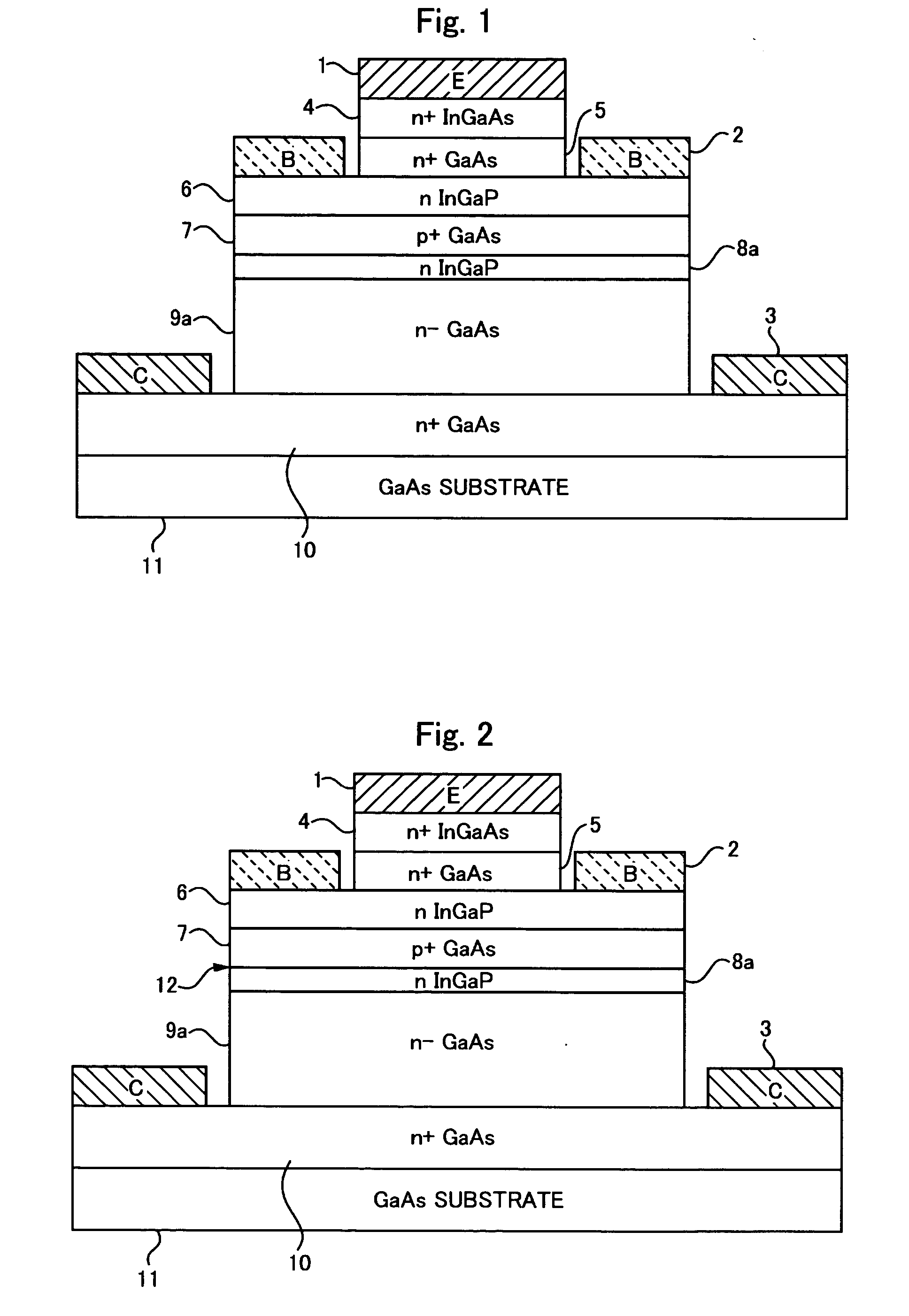
[0051] Embodiment 2, based on the second aspect, is explained using FIG. 2. In Embodiment 2, an N-type In0.48Ga0.52P layer 5 nm thick, doped with Si to 2×1018 cm−3, is formed as the N-type hole barrier thin film layer 8a on the N-type GaAs collector layer 9a, doped to 5×1015 cm−3. This InGaP layer is ordering-system InGaP with a band gap of 1.85 eV. An 80 nm thick P-type GaAs layer with an acceptor concentration of 4×1019 cm−3 is formed on the N-type hole barrier thin film layer 8a, and P-type δ doping is performed at the interface with the N-type hole barrier thin film layer 8a. The δ-doping sheet concentration of P-type δ-doped region 12 is 1×1012 cm−2. It is seen that the turn-on resistance is reduced, from the 6.1×10⁻⁶ Ω-cm2 when a P-type δ-doped region 12 is not formed, to 5.5×10⁻⁶ Ω-cm2 when a P-type δ-doped region 12 is formed.

embodiment 3

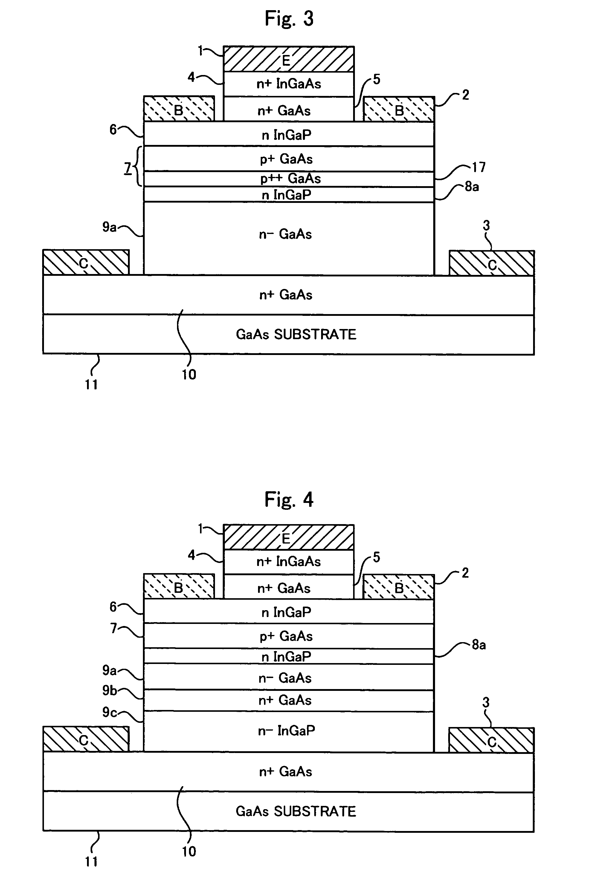
[0052] Embodiment 3, based on the second aspect, is explained using FIG. 3. A difference with the structure shown in FIG. 2 is the insertion, in place of the P-type δ-doped region 12, of a P++ GaAs layer 17. As the P++ GaAs layer 17, GaAs 5 nm thick, doped to 4.2×1019 cm−3, is used. Because other regions of the base layer 7 are doped to 4×1019 cm−3, the increase in the acceptor concentration due to introduction of the P++ GaAs layer 17 is 1×1012 cm−3. The turn-on resistance at this time is 5.5×10⁻⁶ Ω-cm2, so that a low value equivalent to that of Embodiment 2 is obtained.

[0053] (Third Aspect)

[0054] In the first and second aspects of the invention, the N-type hole barrier thin film layer 8a can be configured as an undoped hole barrier thin film layer. This configuration is explained as a third aspect of the invention. Explanation of portions of the configuration which are similar to those of the first and second aspects is omitted. In the third aspect, the N-type hole barrier thin ...


PUM


Abstract

A heterojunction bipolar transistor, having a structure in which a subcollector layer of a first conductive type having a higher doping concentration than a collector layer, a collector layer of the first conductive type, a base layer of the second conductive type, and an emitter layer of the first conductive type are deposited, in order, on a semi-insulating semiconductor substrate, and in which a hole barrier layer of semiconductor material with a band gap wider than that of the base layer is inserted between the base layer and the collector layer, so as to be in direct contact with the base layer.

Description

BACKGROUND OF THE INVENTION [0001] 1. Field of the Invention [0002] This invention relates to a bipolar transistor, and in particular to a heterojunction type bipolar transistor with reduced offset voltage, reduced turn-on resistance, and improved efficiency as a power amplifier in portable terminals. [0003] 2. Description of Related Art [0004] Technological advances in recent years have been attended by the growing use of heterojunction bipolar transistors (HBTs) as power transistors for portable terminals. In order to lengthen the usage time of batteries in portable terminals, it is important that the power-added efficiency of power transistors for portable terminals be improved. In the current-voltage characteristics of an HBT, there exists a region in which, when the collector-emitter voltage VCE is near 0 V, a collector current IC does not flow even if VCE is increased; by reducing this region, the HBT power-added efficiency can be greatly improved. The highest VCE at which IC ...

Claims


Application Information

Patent Timeline
Patent Type & Authority Applications(United States)
IPC IPC(8): H01L21/331H01L29/08H01L29/10H01L29/737
CPCH01L29/0821H01L29/7371H01L29/1004
Inventor NIWA, TAKAKI
Owner RENESAS ELECTRONICS CORP
Why Eureka
Try Eureka