Semiconductor thin film and method of fabricating semiconductor thin film, apparatus for fabricating single crystal semiconductor thin film, and method of fabricating single crystal thin film, single crystal thin film substrate, and semiconductor device

Inactive Publication Date: 2005-05-19
SONY CORP
View PDF34 Cites 27 Cited by
  • Summary
  • Abstract
  • Description
  • Claims
  • Application Information

AI Technical Summary

Benefits of technology

[0036] With these configurations, after hydrogen is removed, the second heat-treatment is continuously performed. Accordingly, it is possible

Problems solved by technology

The method of fabricating the SOI structure, however, requires various steps, for example, a step of sticking single crystal silicon wafers to each other and a step of polishing them, thereby causing disadvantages that the number of steps is increased to prolong the production time, and also the production cost is raised.
In this method, the use of an inexpensive glass substrate may give rise to a problem that the substrate may be deformed or distorted because of its poor heat resistance.
Such an annealing process, however, has a problem that since it takes a long time, the practical utility is poor and also the production cost is raised.
The technique of melting a non-single crystal thin film by irradiation of laser beams emitted from an excimer laser and recrystall

Method used


Image

  • Semiconductor thin film and method of fabricating semiconductor thin film, apparatus for fabricating single crystal semiconductor thin film, and method of fabricating single crystal thin film, single crystal thin film substrate, and semiconductor device
  • Semiconductor thin film and method of fabricating semiconductor thin film, apparatus for fabricating single crystal semiconductor thin film, and method of fabricating single crystal thin film, single crystal thin film substrate, and semiconductor device
  • Semiconductor thin film and method of fabricating semiconductor thin film, apparatus for fabricating single crystal semiconductor thin film, and method of fabricating single crystal thin film, single crystal thin film substrate, and semiconductor device

Examples


first embodiment

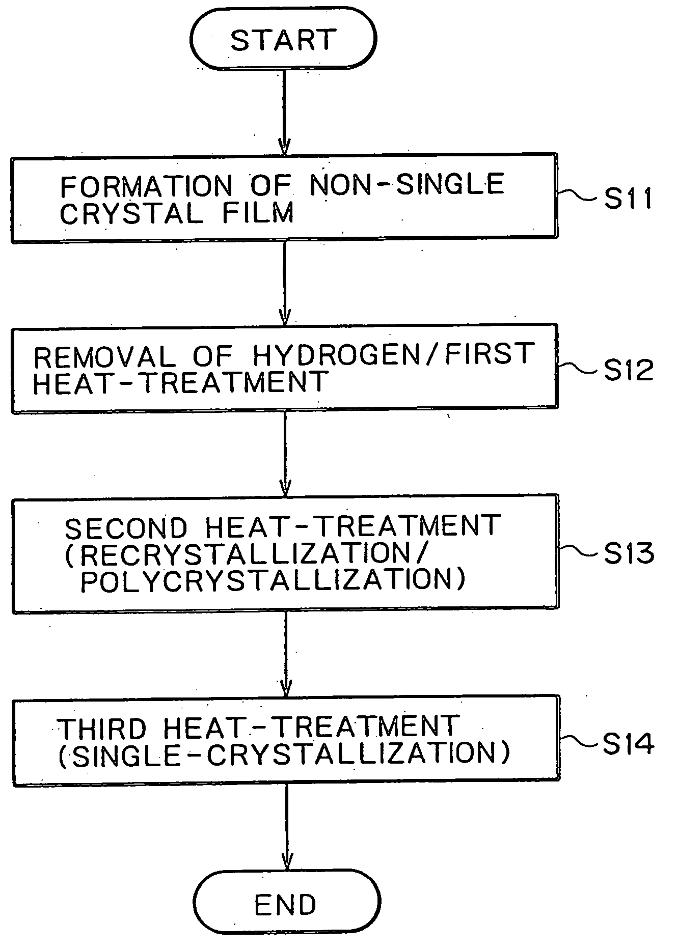
[0065] A method of fabricating a single crystal thin film according to the present invention includes the step of forming a non-single crystal thin film on an insulating base, the step of subjecting the non-single crystal thin film to a first heat-treatment, thereby forming a polycrystalline thin film in which polycrystalline grains are aligned in an approximately regular pattern, and the step of subjecting the polycrystalline thin film to a second heat-treatment, to bond the polycrystalline grains to each other, thereby forming a single crystal thin film.

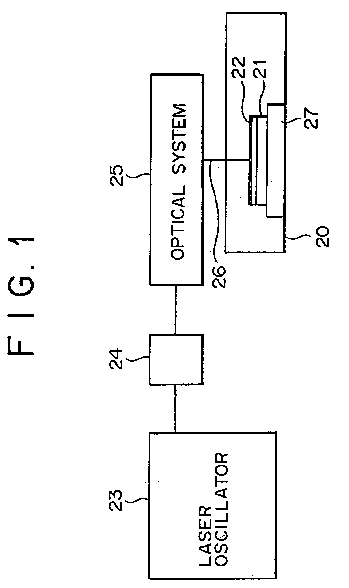
[0066] The method of fabricating a single crystal thin film according to the present invention will be described hereinafter with reference to FIGS. 1 to 6. FIG. 1 shows one example of an excimer laser irradiation apparatus used for the method of fabricating a semiconductor thin film as a single crystal thin film according to the present invention. First, there will be described the excimer laser irradiation apparatus used for irr...

second embodiment

[0083] One example of an active matrix type display as a semiconductor device, which uses a thin film transistor fabricated in accordance with the method of fabricating a single crystal thin film according to the present invention, will be described below with reference to FIG. 7. In this embodiment, a semiconductor device is configured by using a thin film having micro-projections as a channel. Referring to FIG. 7, this display has a panel structure including a pair of insulating substrates 51 and 52, and an electro-optical material 53 held therebetween. For example, a liquid crystal material is used as the electro-optical material 53. A pixel array portion 54 and a drive circuit portion are collectively formed on the lower insulating substrate 51. The drive circuit portion is divided into a vertical scanner 55 and a horizontal scanner 56. Terminal portions 57 for external connection are formed at the upper end of a peripheral portion of the insulating substrate 51. The terminal po...

third embodiment

[0085] A semiconductor thin film in this embodiment is configured as a semiconductor thin film formed on an insulating base, wherein micro-projections are formed on the surface of the semiconductor thin film.

[0086] The semiconductor thin film in this embodiment is also configured as a semiconductor thin film formed, on an insulating base, from a polycrystalline thin film in which polycrystalline grains are aligned in an approximately regular pattern, wherein each micro-projection is formed at a boundary position among at least three or more of the polycrystalline grains.

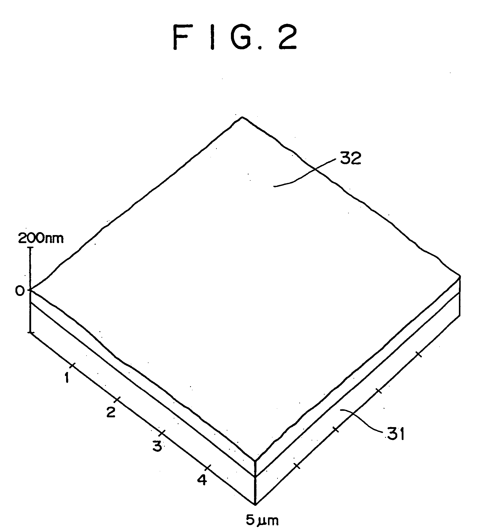
[0087]FIG. 8 is a schematic view of a semiconductor thin film according to the present invention. Referring to FIG. 8, a crystallized thin film 102 is formed on an insulating substrate 101 as an insulating base, and a plurality of micro-projections 103 are formed on the surface of the crystallized thin film 102.

[0088] As the insulating substrate 101, there can be various substrates such as a glass substrate having...


PUM


Abstract

A method of fabricating a single crystal thin film includes forming a non-single crystal thin film on an insulating base; subjecting the non-single crystal thin film to a first heat-treatment, thereby forming a polycrystalline thin film in which polycrystalline grains are aligned in an approximately regular pattern; and subjecting the polycrystalline thin film to a second heat-treatment, thereby forming a single crystal thin film in which the polycrystalline grains are bonded to each other. In this method, either the first heat-treatment or the second heat-treatment may be performed by irradiation of laser beams, preferably, emitted from an excimer laser. A single crystal thin film formed by this fabrication method has a performance higher than a related art polycrystalline thin film and is suitable for fabricating a device having stable characteristics. The single crystal thin film can be fabricated for a short-time by using laser irradiation as the heat-treatments.

Description

BACKGROUND OF THE INVENTION [0001] The present invention relates to a semiconductor thin film applicable to thin film transistors (TFTs) used for liquid crystal displays, memories, and other electronic devices and a fabrication method thereof; an apparatus for fabricating a single crystal semiconductor thin film; and a method of fabricating a single crystal thin film, a single crystal thin film substrate, and a semiconductor device using the substrate. [0002] As semiconductor thin films such as silicon thin films formed on insulating substrates, there have been known an SOI (Silicon On Insulator) structure, and amorphous silicon thin films or polycrystalline silicon thin films formed on glass substrates which have been practically used for liquid crystal displays. [0003] The SOI structure is often formed by way of various steps including a step of sticking single crystal silicon wafers to each other and a step of polishing them, and since the SOI structure basically uses a single cr...

Claims


Application Information

Patent Timeline
IPC IPC(8): C30B1/00H01L21/20
CPCC30B1/00H01L21/2026C30B29/06H01L21/02686H01L21/02422H01L21/02678H01L21/02532H01L21/02609H01L21/0242H01L21/02595H01L21/02689H01L21/02381H01L21/02691H01L21/02598
Inventor SATO, JUNICHIUSUI, SETSUOSAKAMOTO, YASUHIROMORI, YOSHIFUMINAKAJIMA, HIDEHARU
Owner SONY CORP
Why Eureka
Try Eureka