Planar integrated circuit including a plasmon waveguide-fed schottky barrier detector and transistors connected therewith
- Summary
- Abstract
- Description
- Claims
- Application Information
AI Technical Summary
Benefits of technology
Problems solved by technology
Method used
Image

Examples
Embodiment Construction
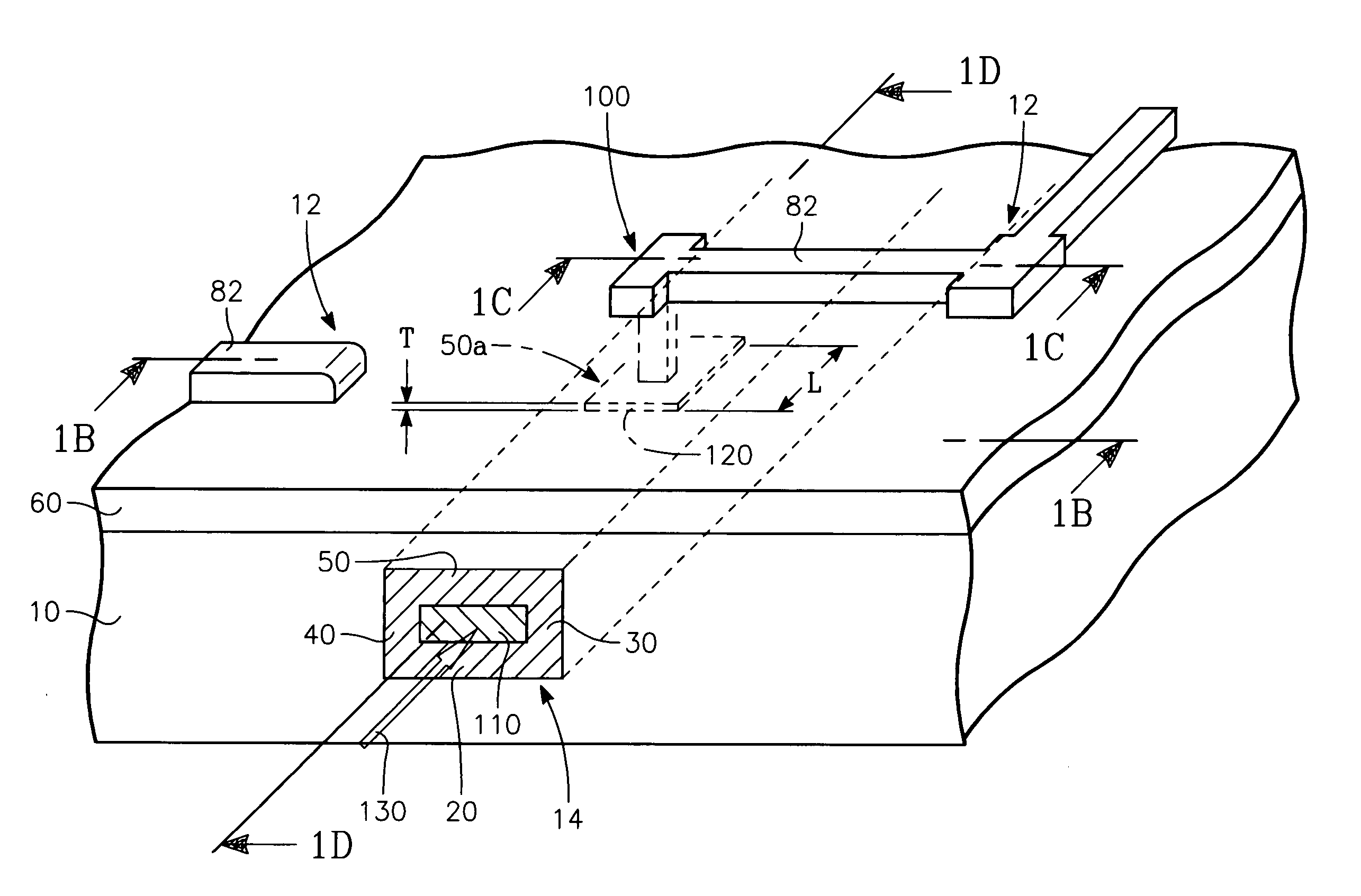
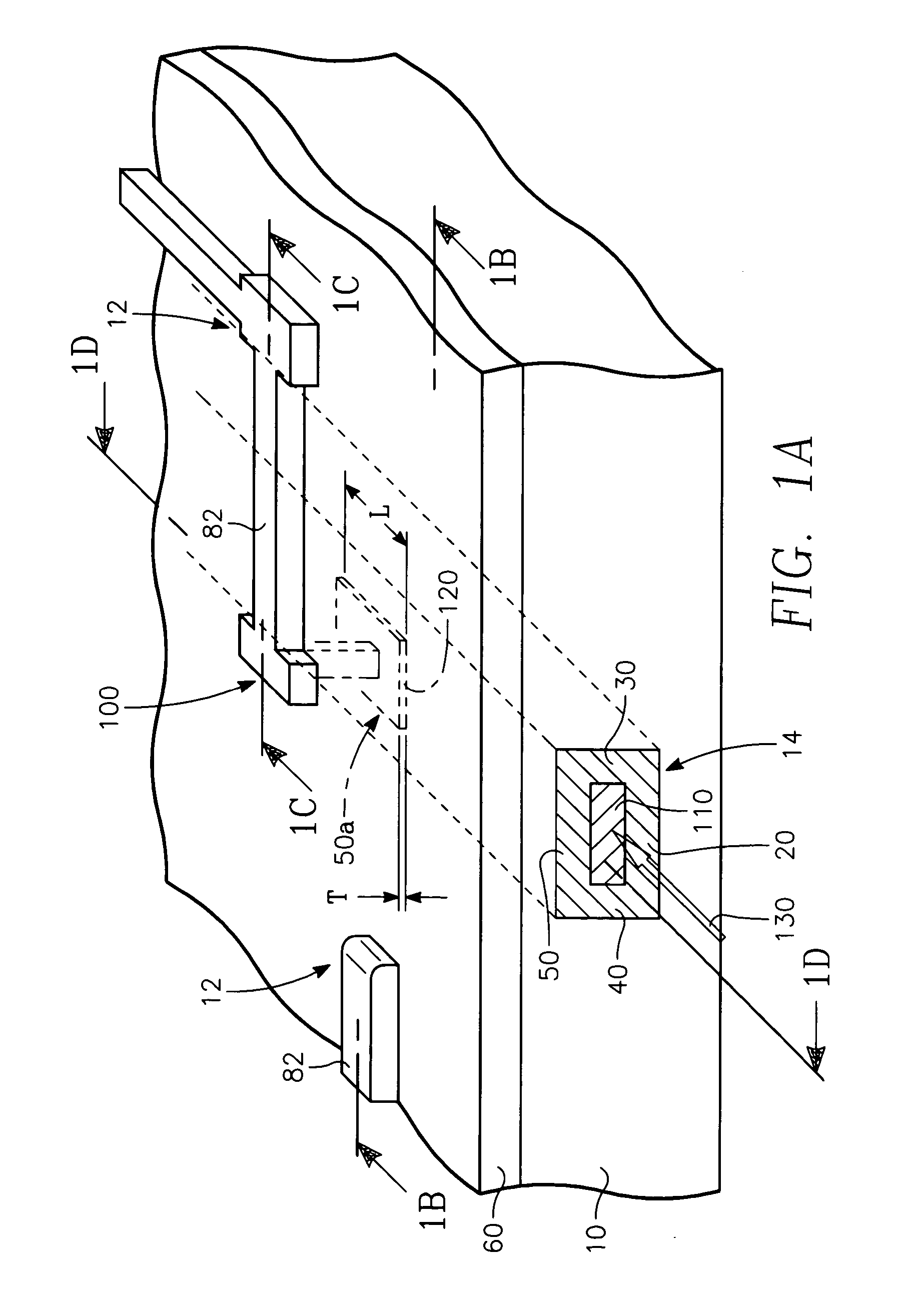
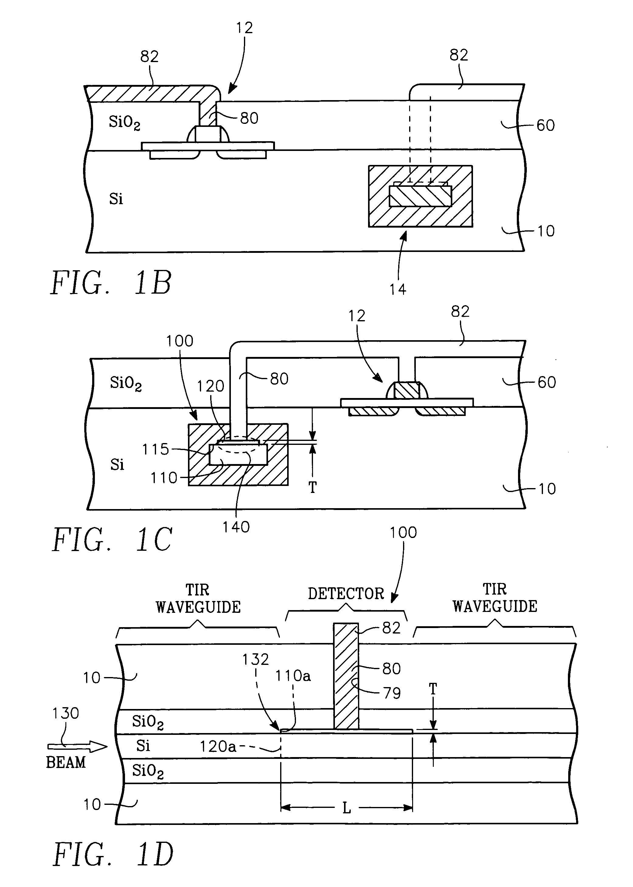
[0025] Referring to FIGS. 1A through FIGS. 1D, a VLSI integrated circuit having a planar structure is formed on a semiconductor substrate 10 including plural transistors 12 formed therein and a buried elongate optical waveguide 14 at least generally beneath the top surface of the semiconductor substrate 10. The semiconductor substrate 10 is typically a silicon wafer, although the substrate 10 may be a silicon layer formed on a semiconductor wafer. The waveguide 14 is a total internal reflection (TIR) waveguide. It consists of an elongate medium or semiconductor layer 110 surrounded on its four sides by a horizontal base layer 20 formed on the substrate 10, a pair of parallel elongate vertical wall layers 30, 40 extending up from the base layer 20, and a ceiling layer 50. The medium, semiconductor layer or core 110 has a different (e.g., higher) index of refraction than the surrounding walls / layers 20, 30, 40, 50. If the elongate core or medium 110 is a semiconductor such as silicon ...
PUM
 Abstract
Description
Claims
Application Information
 - Generate Ideas
- Intellectual Property
- Life Sciences
- Materials
- Tech Scout
- Unparalleled Data Quality
- Higher Quality Content
- 60% Fewer Hallucinations
Browse by: Latest US Patents, China's latest patents, Technical Efficacy Thesaurus, Application Domain, Technology Topic, Popular Technical Reports.
© 2025 PatSnap. All rights reserved.Legal|Privacy policy|Modern Slavery Act Transparency Statement|Sitemap|About US| Contact US: help@patsnap.com