Method for growing group-III nitride semiconductor heterostructure on silicon substrate

a technology of nitride and semiconductors, applied in the field of semiconductor structures, can solve the problems of reducing the application range of gan-on-sic, so as to prevent the formation of amorphous or polycrystalline sinx layers

Inactive Publication Date: 2005-05-19
NATIONAL TSING HUA UNIVERSITY
View PDF3 Cites 45 Cited by
  • Summary
  • Abstract
  • Description
  • Claims
  • Application Information

AI Technical Summary

Benefits of technology

[0011] Moreover, the present invention provides a method for forming a group-III heteroepitaxial structure on a Si(111) substrate. The key feature of the present invention is that the multiple-layer buffer is formed on the Si(111) substrate. The multiple-layer buffer comprises a single-crystal silicon nitride (Si3N4) layer that is formed on the Si(111) substrate by introducing reactive...

Problems solved by technology

At present, the major barrier for widespread applications of nitrides is the lack of perfectly lattice-matched substrates for epitaxial growth.
But, besides the large lattice mismatch, the insulating nature of sapphire renders the processing of nitride devices more difficult and costly.
On the other hand, the high price and limited size of silicon carbide also make the widespread GaN-on-SiC applications difficult.
Therefore, the inter-diffusion...

Method used


Image

  • Method for growing group-III nitride semiconductor heterostructure on silicon substrate
  • Method for growing group-III nitride semiconductor heterostructure on silicon substrate
  • Method for growing group-III nitride semiconductor heterostructure on silicon substrate

Examples


Embodiment Construction

[0019] Some sample embodiments of the invention will now be described in greater detail. Nevertheless, it should be recognized that the present invention can be practiced in a wide range of other embodiments besides those explicitly described, and the scope of the present invention is expressly not limited except as specified in the accompanying claims.

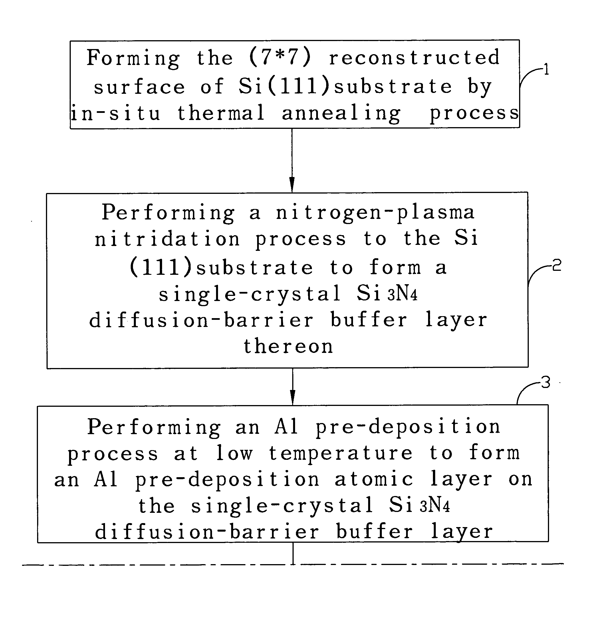
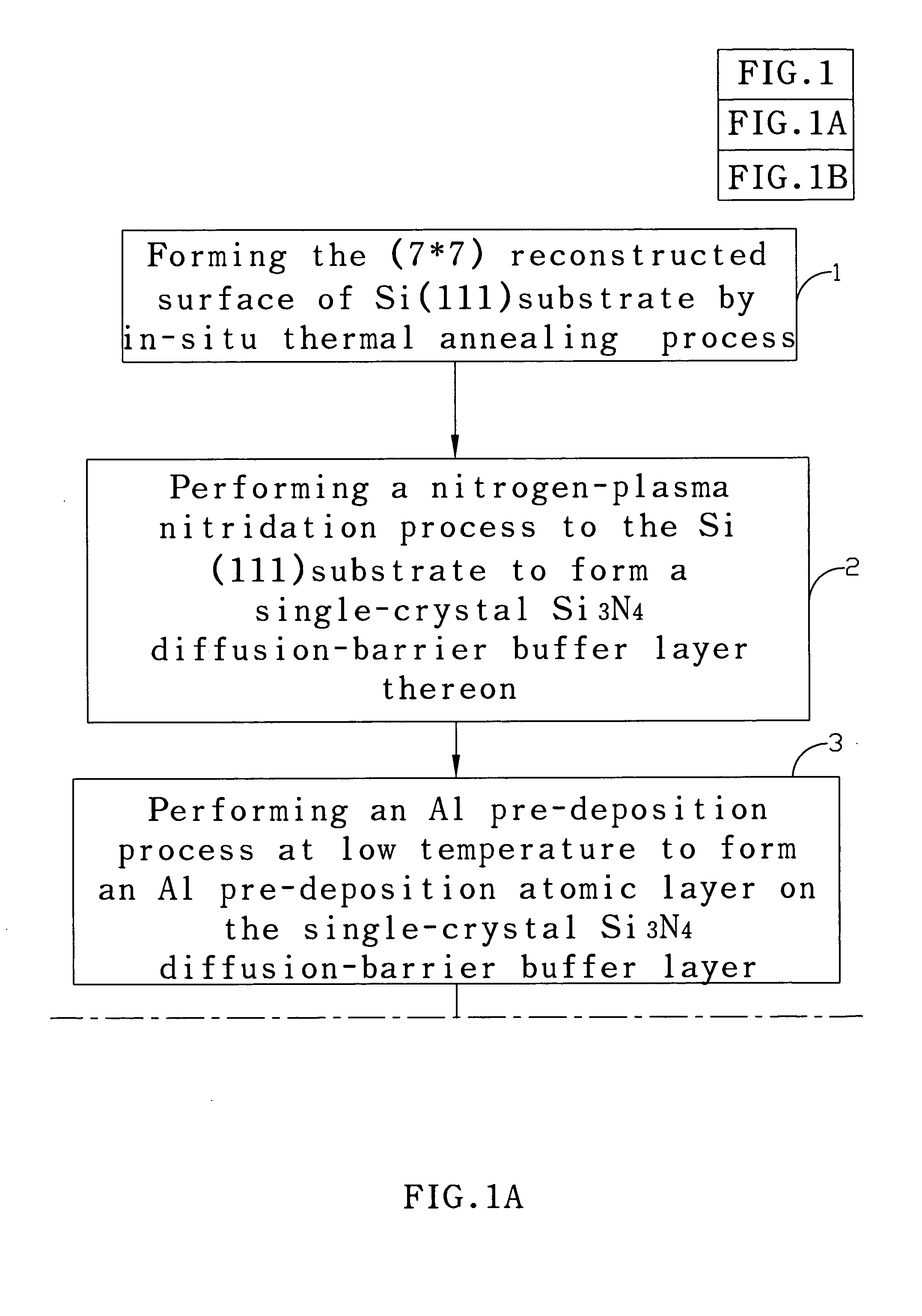
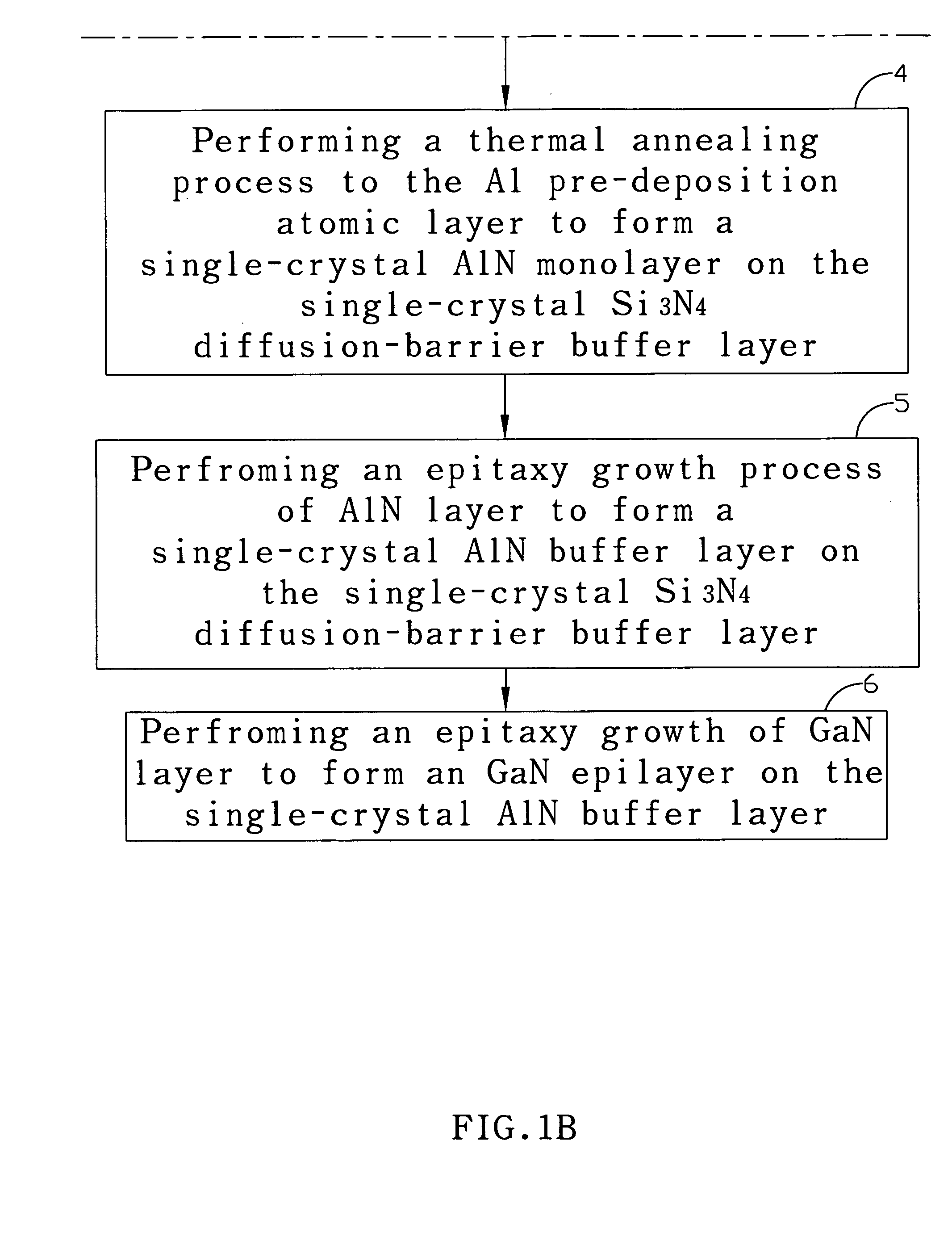
[0020] According to the present invention is to provide a method and a stacked buffer structure for improving the inter-diffusion issue that occurs between AlN / Si, GaN / Si, and InN.

[0021] Group-III nitrides on silicon heteroepitaxy have recently demonstrated to be a viable alternative for growing high-quality group-III nitride films for optoelectronic, electronic, and surface acoustic wave device applications. Besides the availability of lager size (up to 12 inch in diameter), low cost, and excellent crystal quality of Si substrates, Si also possesses excellent material properties such as doping properties (amphoteric type and high c...


PUM


Abstract

The present invention provides a method for growing group-III nitride semiconductor heteroepitaxial structures on a silicon (111) substrate by using a coincidently matched multiple-layer buffer that can be grown on the Si(111) substrate. The coincidently matched multiple-layer buffer comprises a single-crystal silicon nitride (Si3N4) layer that is formed in a controlled manner by introducing reactive nitrogen plasma or ammonia to the Si(111) substrate at a suitably high temperature. Then, an AlN buffer layer or other group-III nitride buffer layer is grown epitaxially on the single-crystal silicon nitride layer. Thereafter, the GaN epitaxial layer or group-III semiconductor heteroepitaxial structure can be grown on the coincidently matched multiple-layer buffer.

Description

BACKGROUND OF THE INVENTION [0001] 1. Field of the Invention [0002] The present invention generally relates to a semiconductor structure, and more particularly to a method for growing a group-III nitride semiconductor heteroepitaxial structure on a silicon substrate. [0003] 2. Description of the Prior Art [0004] The structure of semiconductor light-emitting diode (LED) comprises a substrate, a light emitting structure, and a pair of electrode for powering the diode. The substrate can be opaque or transparent. Light emitting diodes that are based on gallium nitride compounds generally comprise: a transparent, insulating substrate, e.g., a sapphire substrate. To overcome the difficulty of the substantial lattice mismatch between an insulating substrate, e.g., a sapphire substrate, and GaN compound semiconductor, it is a common practice to provide a thin buffer layer or nucleation layer on the sapphire substrate, which is followed by a layer on which an LED structure is grown. Growth o...

Claims


Application Information

Patent Timeline
IPC IPC(8): H01L21/28
CPCH01L21/02381H01L21/02458H01L21/02488H01L29/045H01L21/0254H01L21/3247H01L21/02502
Inventor GWO, SHANGIR
Owner NATIONAL TSING HUA UNIVERSITY
Why Eureka
Try Eureka