

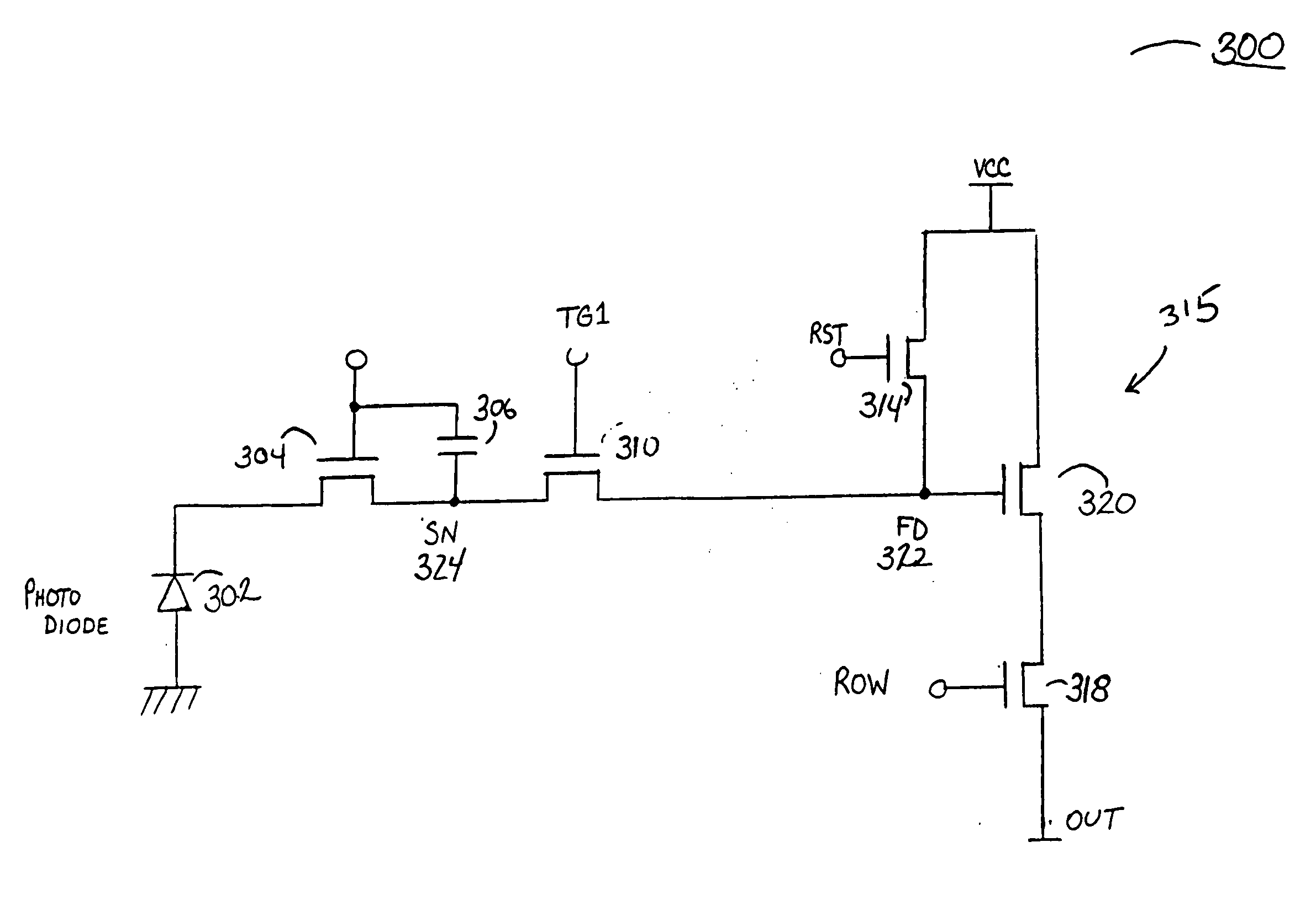
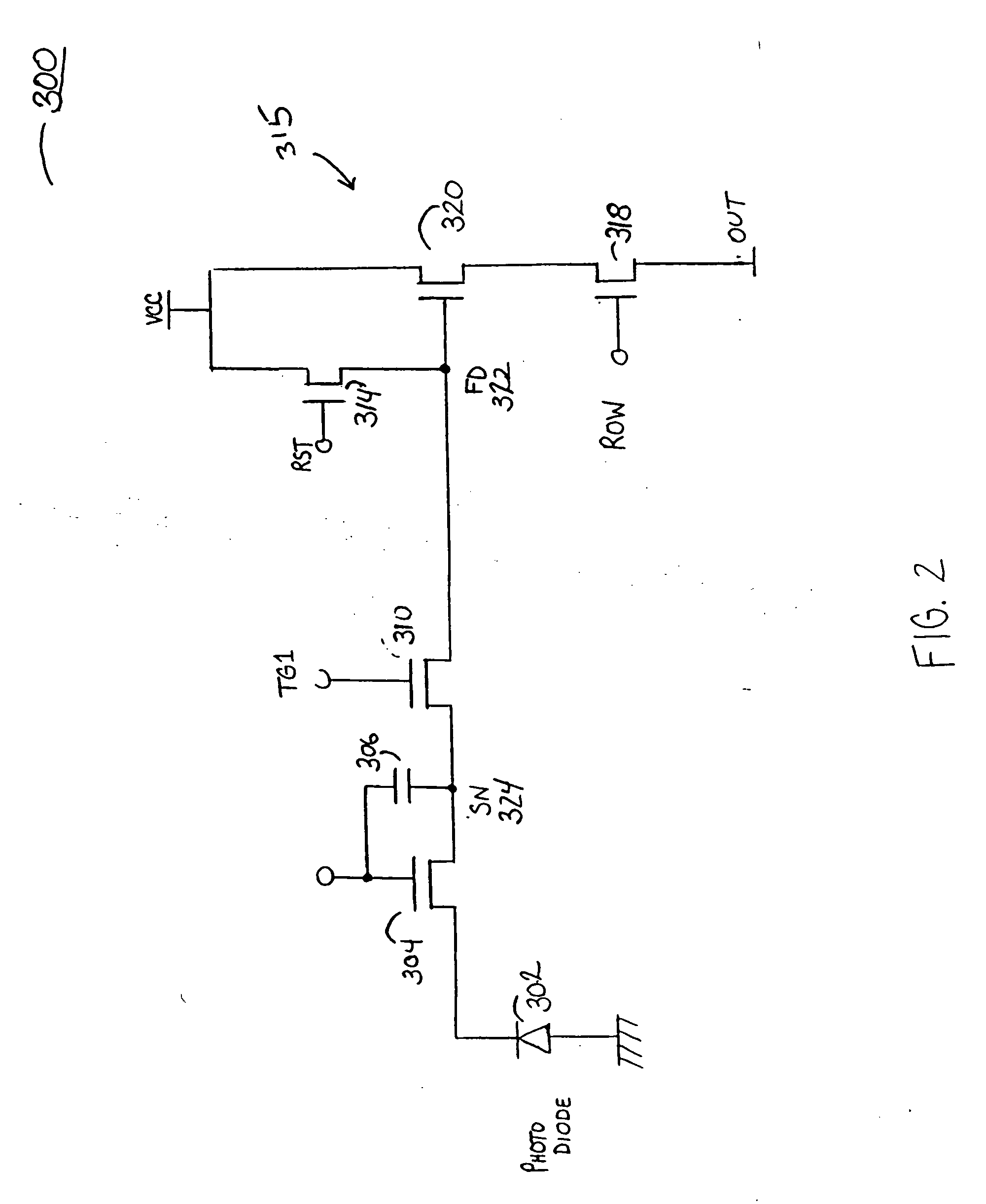
Image sensor with a capacitive storage node linked to transfer gate
a capacitive storage and image sensor technology, applied in the field of improving the charge storage capacity of imager pixels, can solve the problems of increasing the size of the pixel, and low signal to noise ratio of cmos imager pixels, so as to increase the performance of cmos imager embodiments, and increase the charge generating area of each pixel
- Summary
- Abstract
- Description
- Claims
- Application Information
AI Technical Summary
Benefits of technology
Problems solved by technology
Method used
Image

Examples
Embodiment Construction
[0023] In the following detailed description, reference is made to the accompanying drawings, which are a part of the specification, and in which is shown by way of illustration various embodiments whereby the invention may be practiced. These embodiments are described in sufficient detail to enable those skilled in the art to make and use the invention. It is to be understood that other embodiments may be utilized, and that structural, logical, and electrical changes, as well as changes in the materials used, may be made without departing from the spirit and scope of the present invention. Additionally, certain processing steps are described and a particular order of processing steps is disclosed; however, the sequence of steps is not limited to that set forth herein and may be changed as is known in the art, with the exception of steps or acts necessarily occurring in a certain order.
[0024] The terms “wafer” and “substrate” are to be understood as interchangeable and as including...
PUM
 Abstract
Description
Claims
Application Information