Two bit non-volatile electrically erasable and programmable semiconductor memory cell utilizing asymmetrical charge trapping

a semiconductor memory cell and asymmetric charge trapping technology, applied in the field of semiconductor memory devices, can solve the problem that the programing of one of the bits has a very small effect on the other bit, and achieve the effect of slowing down the programming speed of the second bit, reducing the potential drop across the portion of the channel beneath the trapped charge region, and reducing the potential drop across the channel

Inactive Publication Date: 2005-05-26
SAIFUN SEMICON
View PDF99 Cites 31 Cited by
  • Summary
  • Abstract
  • Description
  • Claims
  • Application Information

AI Technical Summary

Benefits of technology

[0030] A novel aspect of the memory device is that while both bits are programmed in the conventional manner, using hot electron programming, each bit is read in a direction opposite that in which it was programmed with a relatively low gate voltage. For example, the right bit is programmed conventionally by applying programming voltages to the gate and the drain while the source is grounded. Hot electrons are accelerated sufficiently to be injected into a region of the trapping dielectric layer near the drain. The device, however, is read in the opposite direction from which it was written, meaning voltages are applied to the gate and the source while the drain is grounded. The left bit is similarly programmed and read by swapping the functionality of source and drain terminals. Programming one of the bits leaves the other bit with its information intact and undisturbed. Programming one of the bits does, however, have a very small effect on the other bit, e.g., slightly slower programming speed for the second bit.
[0038] Considerations of the two bit memory cell of the present invention are described hereinbelow. The first is the fact that reading in the reverse direction permits read through of the trapping region associated with the other bit. The second is that programming the device to a low VT, by clamping the word line voltage VWL, further enhances the margin for each bit. The margin is defined as the parameters that will program one of the bits without affecting the other.

Problems solved by technology

Programming one of the bits does, however, have a very small effect on the other bit, e.g., slightly slower programming speed for the second bit.

Method used


Image

  • Two bit non-volatile electrically erasable and programmable semiconductor memory cell utilizing asymmetrical charge trapping
  • Two bit non-volatile electrically erasable and programmable semiconductor memory cell utilizing asymmetrical charge trapping
  • Two bit non-volatile electrically erasable and programmable semiconductor memory cell utilizing asymmetrical charge trapping

Examples


Embodiment Construction

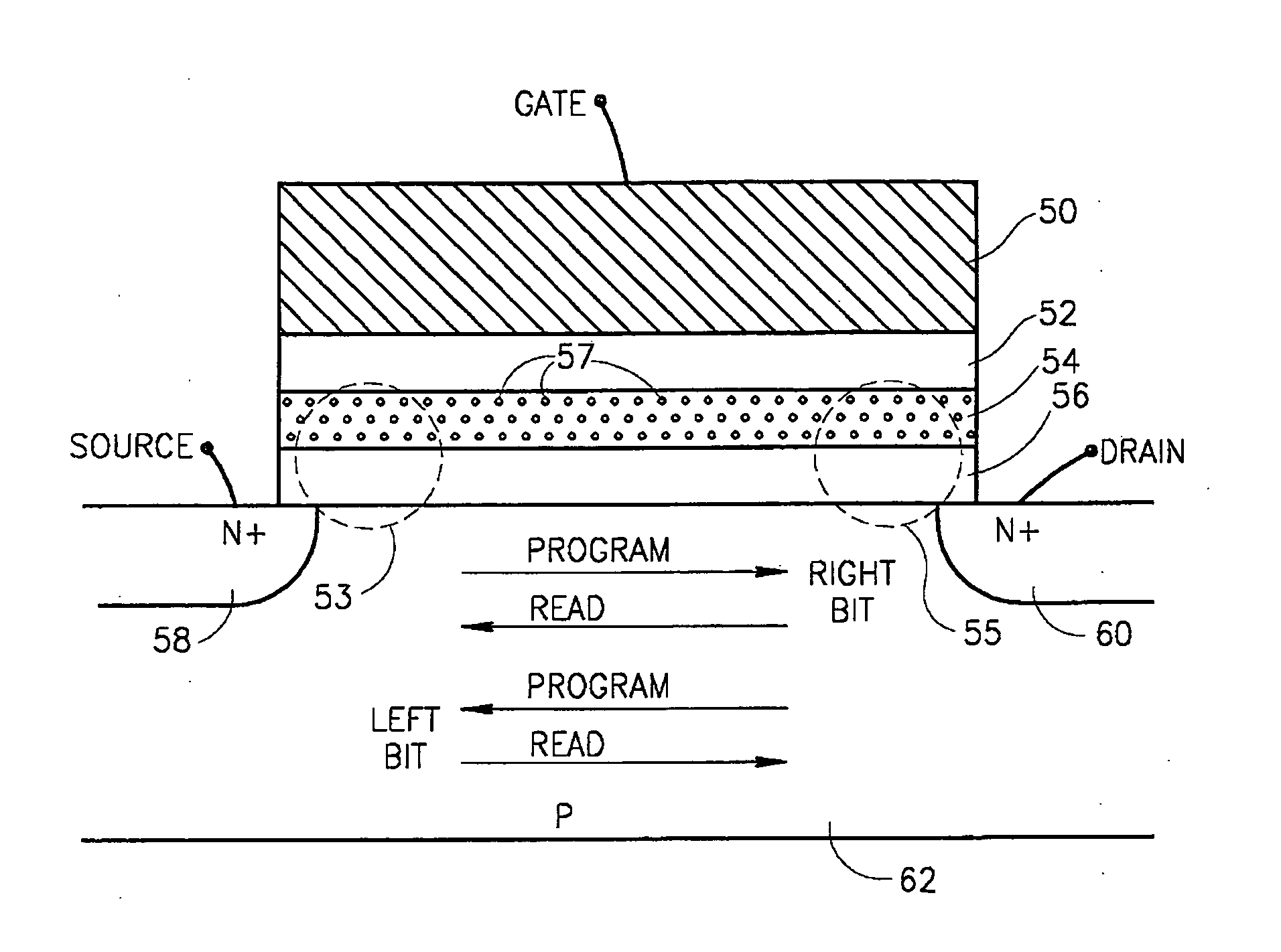
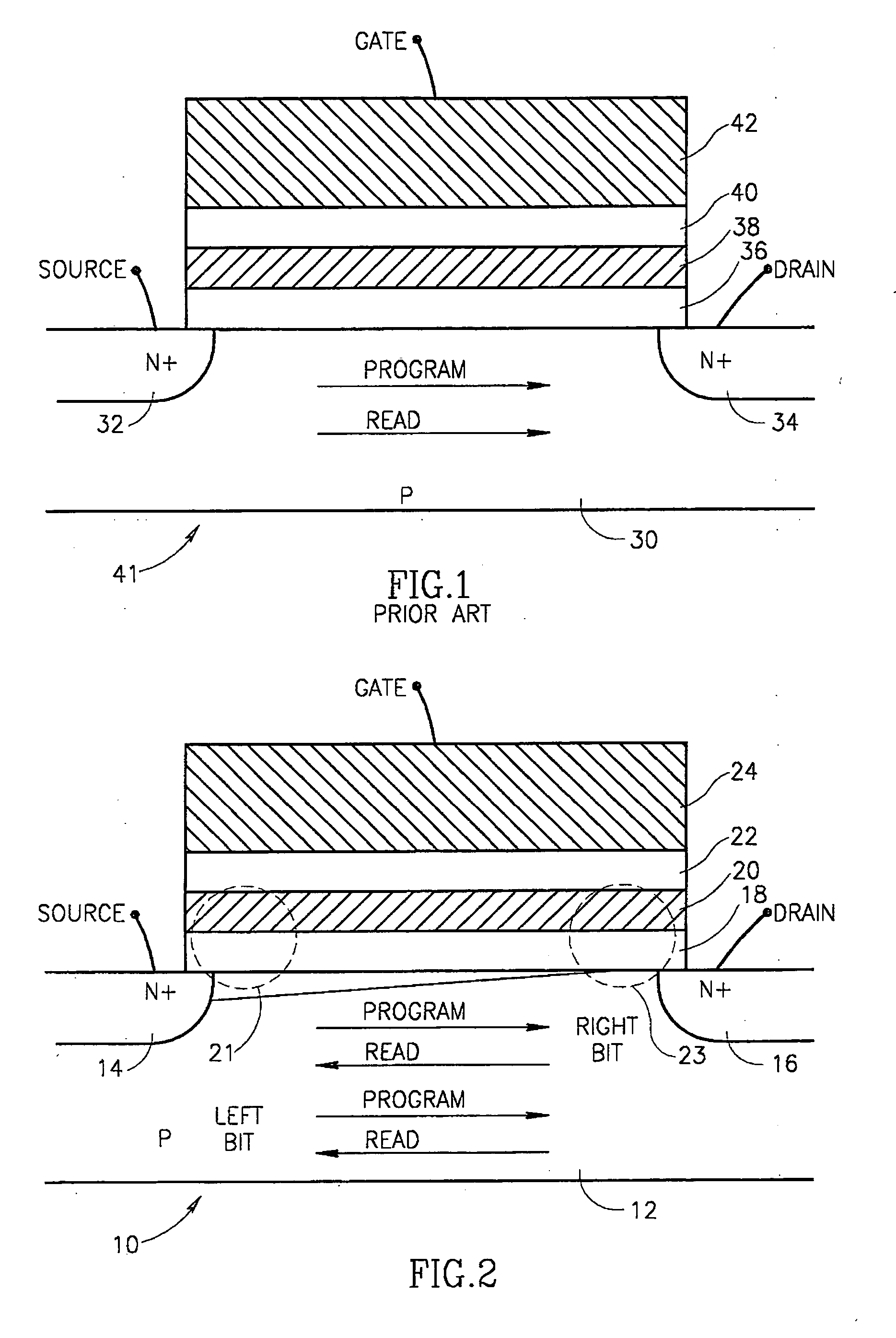
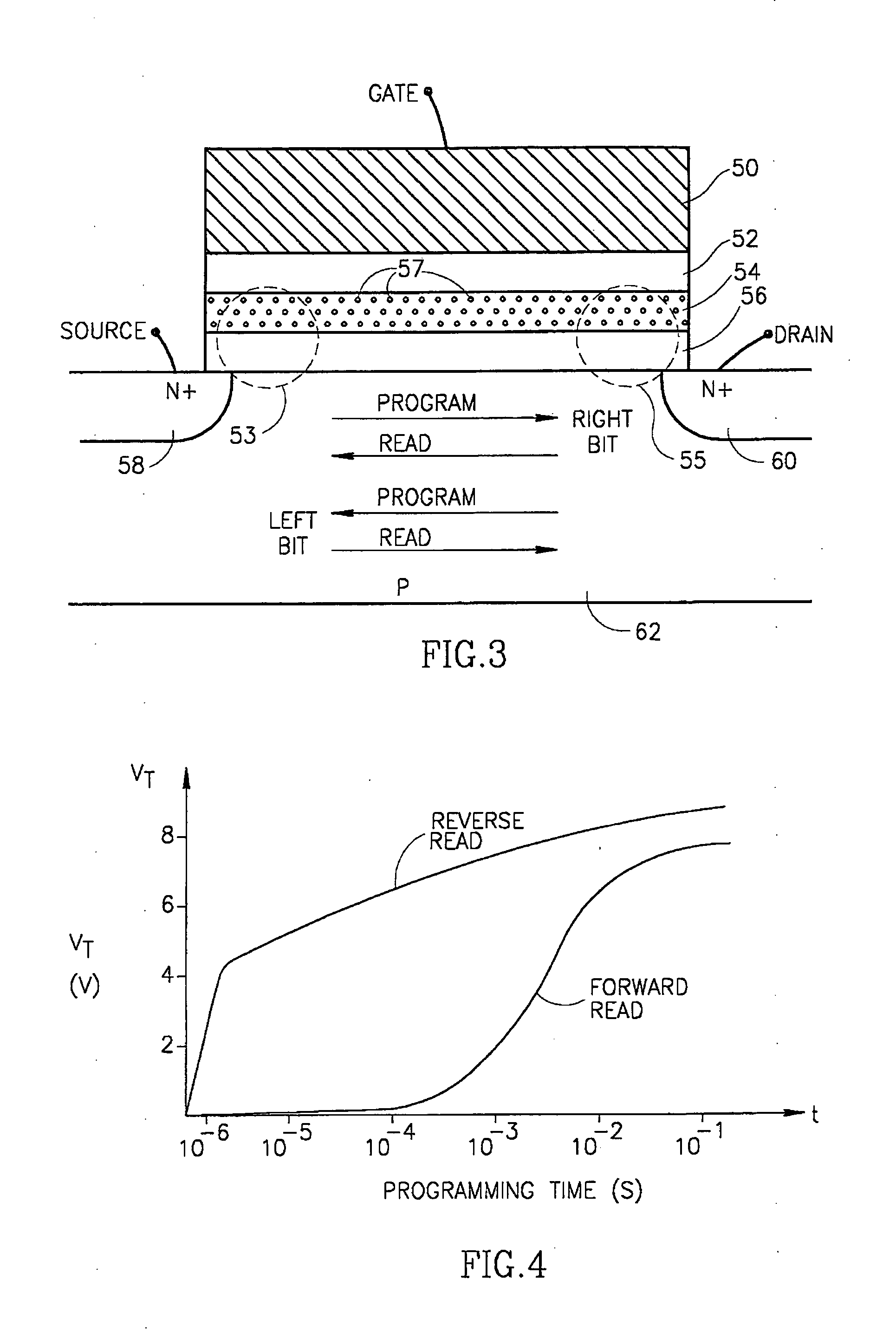
[0069] The two bit flash EEPROM cell of the present invention can best be understood with an understanding of how present day single bit charge trapping dielectric flash EEPROM memory cells are constructed, programmed and read. Thus, prior art single bit ONO EEPROM memory cells and the conventional method used to program, read and erase them are described in some detail. Illustrated in FIG. 1 is a cross section of a conventional ONO EEPROM memory cell as disclosed in the technical article entitled “A True Single-Transistor Oxide-Nitride-Oxide EEPROM Device,” T. Y. Chan, K. K. Young and Chenming Hu, IEEE Electron Device Letters, March 1987, incorporated herein by reference. The memory cell, generally referenced 41, comprises a P-type silicon substrate 30, two PN junctions between N+ source and drain regions 32, 34 and P type substrate 30, a non conducting nitride layer 38 sandwiched between two oxide layers 36, 40 and a polycrystalline conducting layer 42.

Programming Prior Art Sing...


PUM


Abstract

A non-volatile electrically erasable programmable read only memory (EEPROM) capable of storing two bit of information having a nonconducting charge trapping dielectric, such as silicon nitride, sandwiched between two silicon dioxide layers acting as electrical insulators is disclosed. The invention includes a method of programming, reading and erasing the two bit EEPROM device. The nonconducting dielectric layer functions as an electrical charge trapping medium. A conducting gate layer is placed over the upper silicon dioxide layer. A left and a right bit are stored in physically different areas of the charge trapping layer, near left and right regions of the memory cell, respectively. Each bit of the memory device is programmed in the conventional manner, using hot electron programming, by applying programming voltages to the gate and to either the left or the right region while the other region is grounded. Hot electrons are accelerated sufficiently to be injected into the region of the trapping dielectric layer near where the programming voltages were applied to. The device, however, is read in the opposite direction from which it was written, meaning voltages are applied to the gate and to either the right or the left region while the other region is grounded. Two bits are able to be programmed and read due to a combination of relatively low gate voltages with reading in the reverse direction. This greatly reduces the potential across the trapped charge region. This permits much shorter programming times by amplifying the effect of the charge trapped in the localized trapping region associated with each of the bits. In addition, both bits of the memory cell can be individually erased by applying suitable erase voltages to the gate and either left or right regions so as to cause electrons to be removed from the corresponding charge trapping region of the nitride layer.

Description

FIELD OF THE INVENTION [0001] The present invention relates generally to semiconductor memory devices and more particularly to multi-bit flash electrically erasable programmable read only memory (EEPROM) cells that utilize the phenomenon of hot electron injection to trap charge within a trapping dielectric material within the gate. BACKGROUND OF THE INVENTION [0002] Memory devices for non-volatile storage of information are currently in widespread use today, being used in a myriad of applications. A few examples of non-volatile semiconductor memory include read only memory (ROM), programmable read only memory (PROM), erasable programmable read only memory (EPROM), electrically erasable programmable read only memory (EEPROM) and flash EEPROM. [0003] Semiconductor ROM devices, however, suffer from the disadvantage of not being electrically programmable memory devices. The programming of a ROM occurs during one of the steps of manufacture using special masks containing the data to be s...

Claims


Application Information

Patent Timeline
Patent Type & Authority Applications(United States)
IPC IPC(8): G11C11/56G11C16/04H01L21/8247G11C16/10G11C16/14G11C16/26H01L27/105H01L29/788H01L29/792
CPCG11C11/5671G11C16/0475G11C16/10G11C16/14H01L29/7923H01L21/28282H01L29/7885H01L29/7887G11C16/26H01L29/40117
Inventor EITAN, BOAZ
Owner SAIFUN SEMICON
Why Eureka
Try Eureka