Polishing apparatus

a technology of polishing apparatus and rotary blade, which is applied in the direction of grinding machine components, manufacturing tools, lapping machines, etc., can solve the problems of large rc delay, increased semiconductor devices, and large delay in electric signals of semiconductor devices, so as to achieve the effect of broadening the process margin

Inactive Publication Date: 2005-05-26
EBARA CORP +1
View PDF7 Cites 24 Cited by
  • Summary
  • Abstract
  • Description
  • Claims
  • Application Information

AI Technical Summary

Benefits of technology

[0032] According to the present invention, even if a material having a weak adhesion such as a low dielectric constant material is used for a film of a semiconductor device, the film formed on the substrate can be prevented from being peeled off during polishing of the substrate. Further, it is not necessary to select the excessively safe process which takes long time to polish the substrate in order to prevent the film from being peeled off. Thus, the process margin can be broadened.

Problems solved by technology

However, as a semiconductor device has become smaller in size and more highly integrated, an electric signal delay in the semiconductor device, i.e., RC delay has become a large problem.
Further, as a semiconductor device has become smaller in size and more highly integrated, structures of semiconductor elements have become more complicated.
Accordingly, irregularities on a surface of a semiconductor device become increased, and hence step heights on the surface of the semiconductor device tend to be larger.
Further, an open circuit is caused by disconnection of interconnects, or a short circuit is caused by insufficient insulation between interconnect layers.
As a result, good products cannot be obtained, and the yield tends to be reduced.
Furthermore, even if a semiconductor device initially works normally, reliability of the semiconductor device is lowered after a long-term use.
Therefore, if the irregularities of the surface of the semiconductor device are increased, then it becomes difficult to form a fine pattern on the semiconductor device.
Therefore, in a case where the low dielectric constant material is used for the interlayer dielectric / intermetal dielectric, the following problems may arise in a polishing process: (1) Separation (peeling-off) occurs at an interface between the interlayer dielectric / intermetal dielectric and a metal film or other films, resulting in failure of a fabrication process of a semiconductor device.
(2) In order to prevent such separation of the interlayer dielectric / intermetal dielectric, an excessively low polishing pressure is required in the polishing process, thus increasing a process time in a polishing process.

Method used


Image

  • Polishing apparatus
  • Polishing apparatus
  • Polishing apparatus

Examples


Embodiment Construction

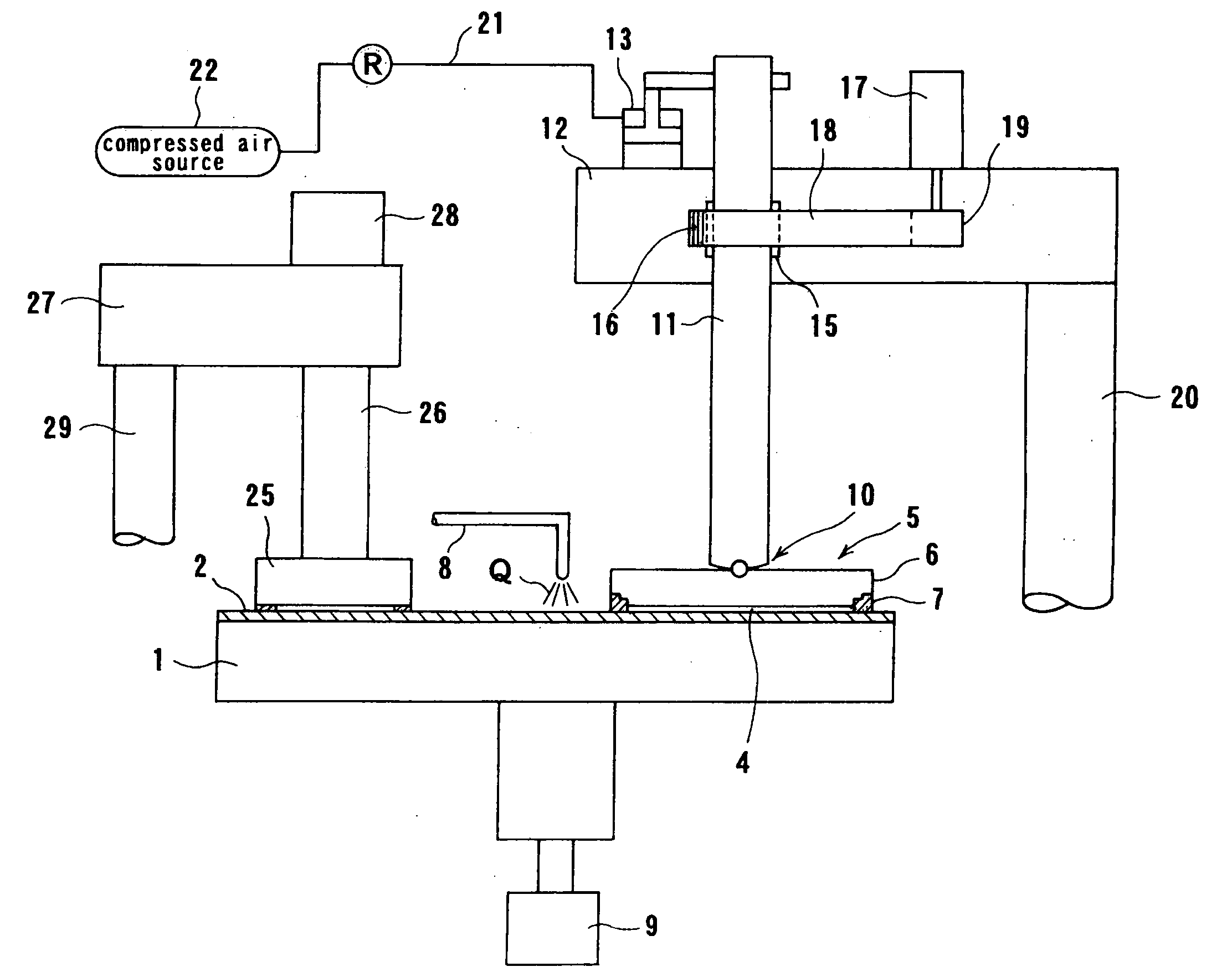
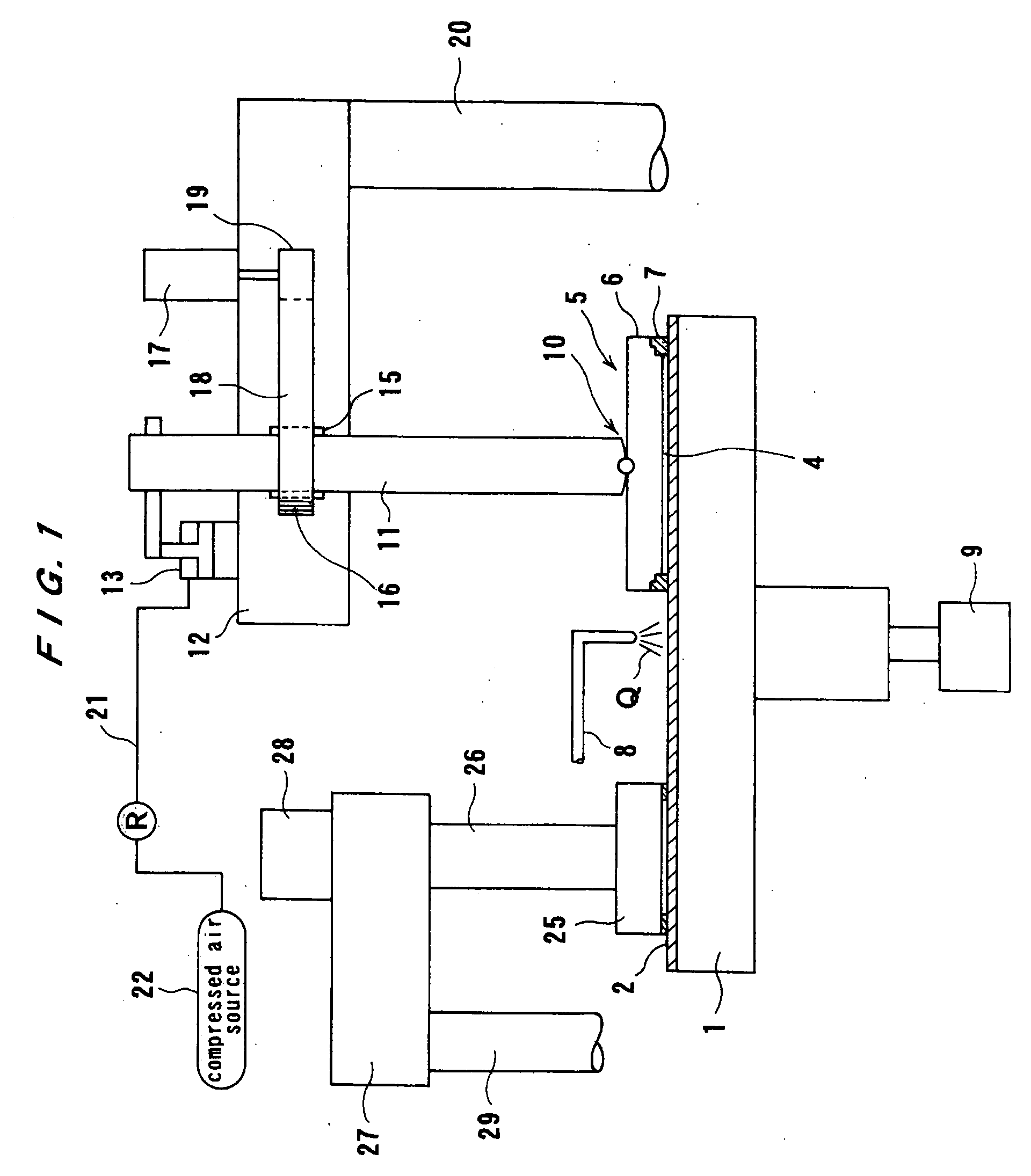
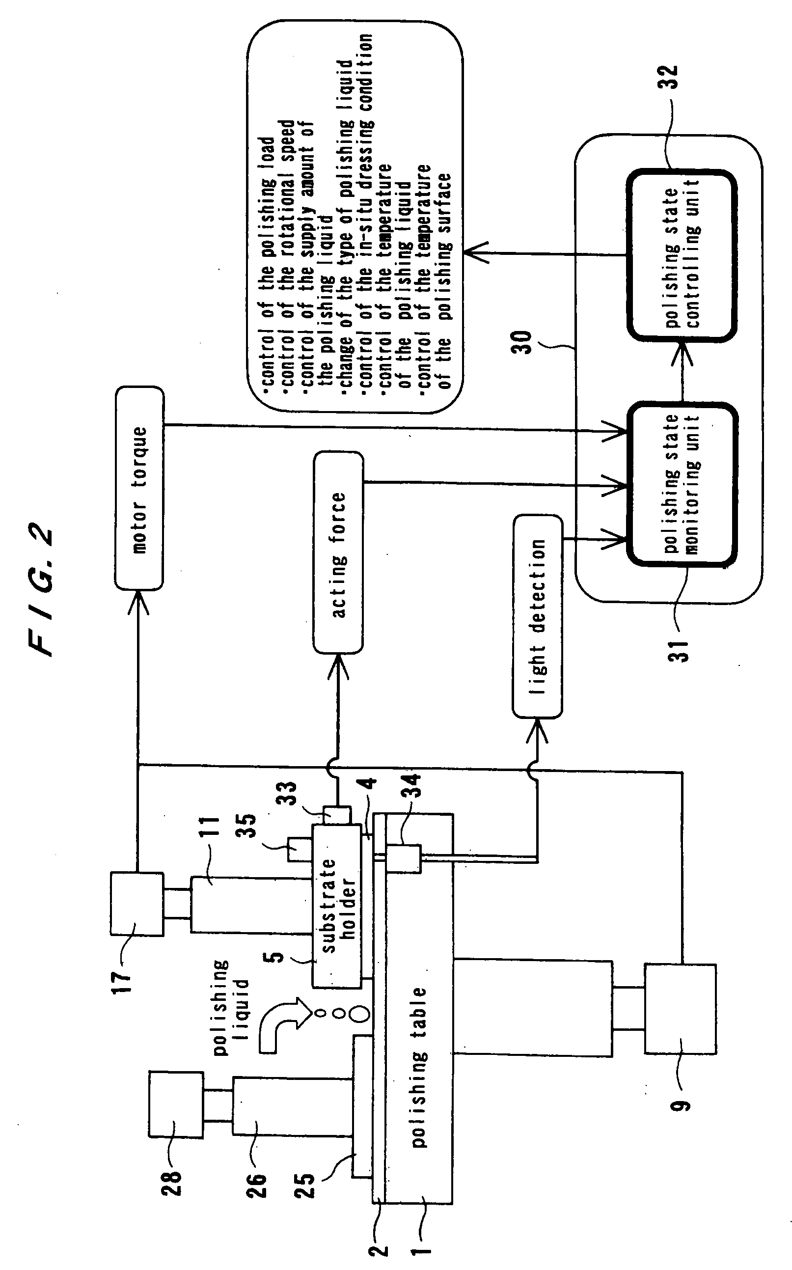
[0039] A polishing apparatus according to embodiments of the present invention will be described below with reference to drawings.

[0040]FIG. 1 is a schematic view showing an overall structure of a polishing apparatus according to an embodiment of the present invention. As shown in FIG. 1, the polishing apparatus according to the present invention comprises a polishing table 1 having a polishing surface, a substrate holder 5 for holding a substrate 4 such as a semiconductor wafer to be polished and pressing the substrate 4 against the polishing surface of the polishing table 1, and a dresser 25 for dressing the polishing surface of the polishing table 1. The substrate 4 to be polished has a lower surface comprising a low-k film which is an object to be polished. A material for forming the low-k film includes SiOC, F doped SiO2, HSQ, MSQ, BCB (Benzo Cyclo Butene), PAE (Poly Arylene Ethers), SiO2, SiOF, Polyimide, PSI (Polyimide siloxane), CVD-PI (CVD polyimide), PTFE (Polytetrafluoro...


PUM


Abstract

A polishing apparatus is used for polishing a substrate such as a semiconductor wafer to a flat finish. The polishing apparatus includes a polishing tool having a polishing surface, a substrate holder configured to hold a substrate, a monitoring device configured to monitor a polishing state of the surface of the substrate being polished, and a controlling device configured to change a polishing condition on the basis of the polishing state of the surface of the substrate being polished detected by the monitoring device.

Description

BACKGROUND OF THE INVENTION [0001] 1. Field of the Invention [0002] The present invention relates to a polishing apparatus for polishing a substrate such as a semiconductor wafer to a flat finish. [0003] 2. Description of the Related Art [0004] As telecommunication means such as Internet and high-speed large-capacity communication network have been remarkably developed, there has been an increasing demand for miniaturization and high integration in a semiconductor integrated circuit technology which supports the telecommunication means. [0005] However, as a semiconductor device has become smaller in size and more highly integrated, an electric signal delay in the semiconductor device, i.e., RC delay has become a large problem. The RC delay is determined by the product of interconnect resistance R and interconnect capacitance C. Therefore, a countermeasure for preventing such RC delay is to use a combination of an interconnect metal having a low electric resistance and an interlayer ...

Claims


Application Information

Patent Timeline
Patent Type & Authority Applications(United States)
IPC IPC(8): B24B49/10B24B37/07B24B49/12B24B49/16H01L21/304
CPCB24B49/12B24B37/013
Inventor MATSUO, HISANORIISHIKAWA, AKIRA
Owner EBARA CORP
Why Eureka
Try Eureka