

Semiconductor device and method for manufacturing the same
- Summary
- Abstract
- Description
- Claims
- Application Information
AI Technical Summary
Benefits of technology
Problems solved by technology
Method used
Image

Examples
embodiment mode 1
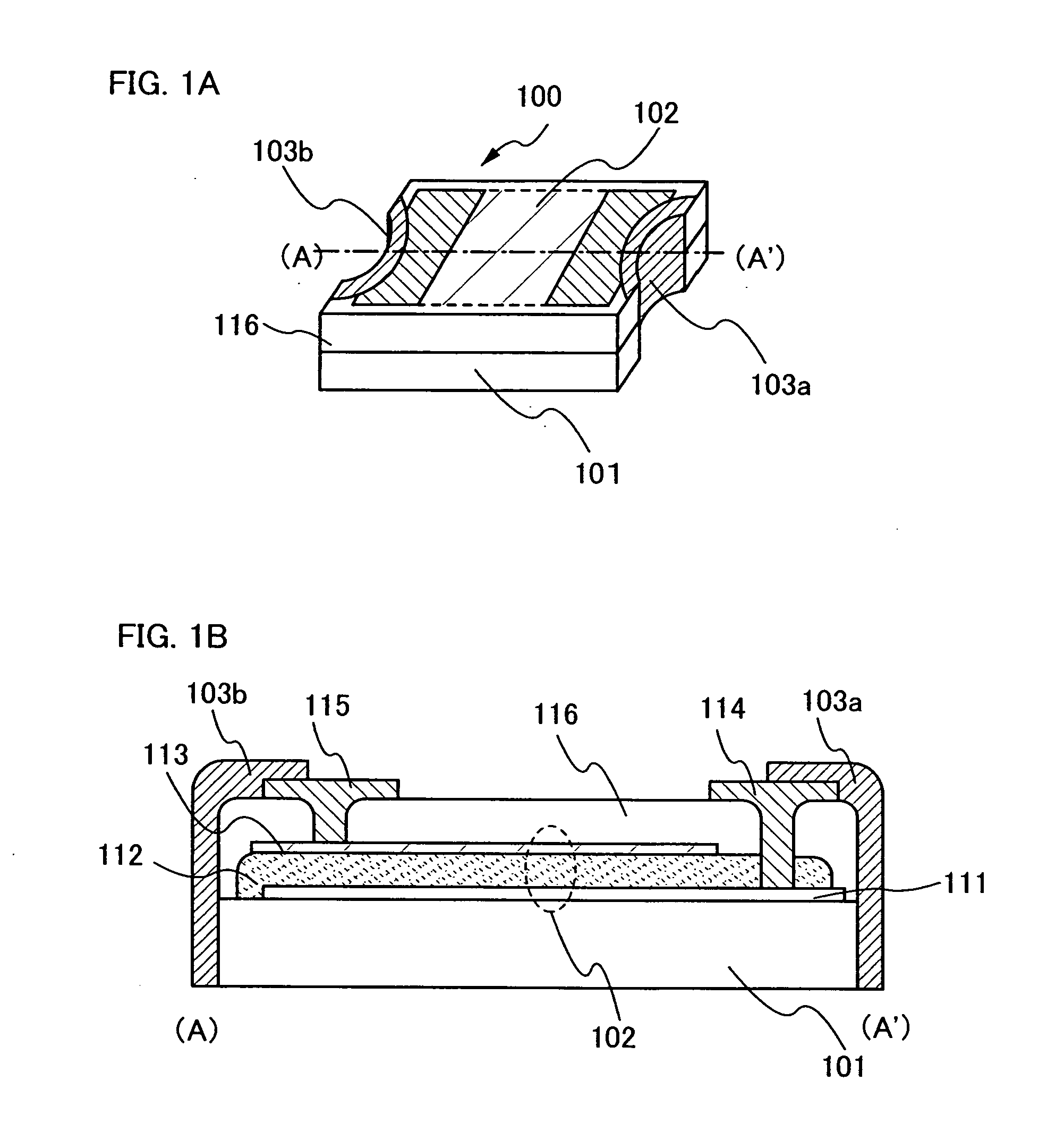
[0044] An optical sensor that is formed over a plastic substrate and that has a concave portion in a side face thereof is described with reference to FIGS. 1A and 1B in this embodiment mode.
[0045]FIG. 1A is an oblique drawing of an optical sensor 100 of the present invention. A semiconductor element 102 is formed over a plastic substrate 101. A side face of the optical sensor 100 has a concave shape, and a conductive film to be connection terminals 103a and 103b is formed in this area.
[0046] The semiconductor element 102 can be integrally formed on the substrate by using a semiconductor film, preferably, a semiconductor thin film, and thus, downsizing and thinning of a semiconductor device can be achieved.
[0047] The concave shape in the side face of the optical sensor is curved in this embodiment mode. Note that the concave shape may have a flat surface. That is to say, the concave shape is a semi cylindrical having a curved surface or a rectangular column having a flat surface. ...
embodiment mode 2
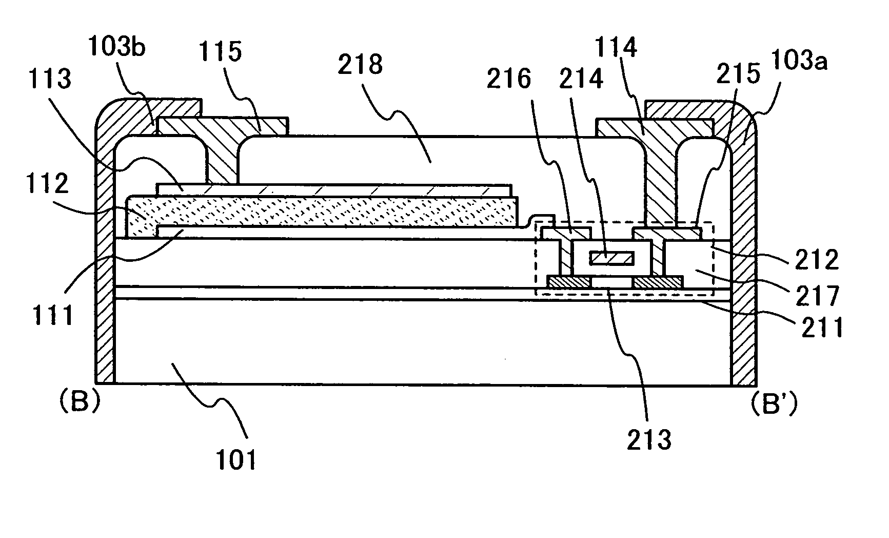
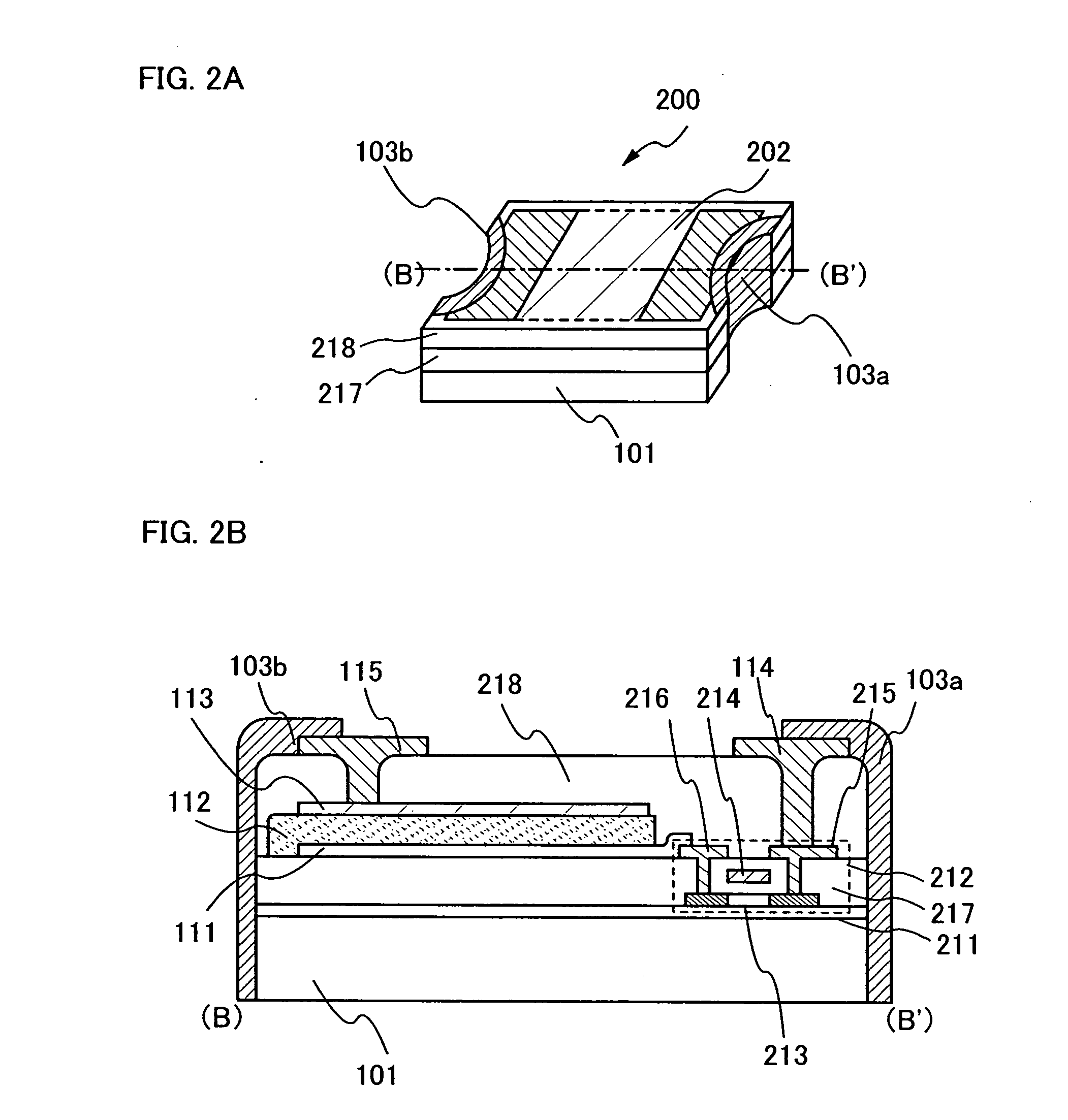
[0064] An optical sensor having a circuit for amplifying current detected in a light-receiving portion is described with reference to FIGS. 2A and 2B. An example of using a thin film transistor (hereinafter, referred to as a TFT) as an element constituting an amplifier circuit is shown, but the present invention is not limited thereto and can employ an operational amplifier (op-amp) and the like.
[0065]FIG. 2A is an oblique drawing of an optical sensor of this embodiment mode. As in Embodiment Mode 1, a semiconductor element 202 is formed on a surface of a plastic substrate 101. A diode or a TFT having such a structure shown in Embodiment Mode 1 can be appropriately applied to the semiconductor element. In addition, a side face of an optical sensor 200 has a concave portion, and a conductive film to be connection terminals 103a and 103b is formed therein. The shape shown in Embodiment Mode 1 can be applied to the shape of the concave portion in the side face of the optical sensor.
[...
embodiment mode 3
[0078] An example of a driver circuit of an optical sensor in Embodiment Mode 2 is shown with reference to FIG. 3. In this embodiment mode, a current mirror circuit is used as an amplifier circuit in the optical sensor.
[0079] Herein, two transistors are connected to each other and one of them is connected to a diode (a light-receiving portion). The TFT connected to a diode 301 is a first TFT 302, and the TFT that is connected to the first TFT in parallel is a second TFT 303. Gate electrodes and source wirings of the first TFT 302 and the second TFT 303 are connected to one another. A drain of the first TFT 302 is connected to a cathode of the diode 301, and an anode of the diode 301 is connected to a drain of the second TFT 303. Sources of the first TFT and the second TFT are connected to VSS 304. The anode of the diode and the drain of the second TFT are connected to VDD 305 that is an output terminal, and brightness of light can be detected by a value of current flowing at the po...
PUM
 Abstract
Description
Claims
Application Information