Ultra-thin Si MOSFET device structure and method of manufacture

Inactive Publication Date: 2005-06-02
GLOBALFOUNDRIES INC
View PDF17 Cites 29 Cited by
  • Summary
  • Abstract
  • Description
  • Claims
  • Application Information

AI Technical Summary

Benefits of technology

[0007] In one prior art thin Si channel device, a wide disposable spacer is utilized to grow the raised source/drain regions. High-energy implants are performed to form deep source/drain regions. Following the high-energy implant, the wide disposable spacer is removed and extension regions are implanted. This prior art process overcomes excessive extension dopant diffusion and the epitaxial Si growth rate differential between p-type and n-type regions, but does not overcome the formation of high resistance regions outside the raised source/drain area, which are key to the performance of thin SOI MOSFETs. The formation of high resistance regions outside the raised source/drain area is also cost ineffective. In addition, the raised source drain regions cause increased parasitic capacitance, which slows down circuit performance.
[0008] Another prior art scheme utilizes a dummy structure as an implant mask for implanting oxygen ions into a bulk Si substrate. This process simultaneously creates a buried oxide layer and also forms a thin Si region; the thin Si region is produced by the dummy structure. However, in order to create a suitably thick buried oxide layer, a high-energy oxygen implant is needed. The large energy distribution of the high-energy implant required to form a suitably thick buried oxide layer disadvantageously results in a substantially wide region of thin Si that is much larger, in a lateral direction, than the desired width of the channel region. The lateral spread of the oxygen implant is proportional to the implant depth. Specifically, the lateral spread for oxygen implants conducted through gate structures into substrates utilized in conventional semiconducting devices is equal to ⅓ the depth of the peak oxygen implant in the vertical direction. The lateral spread is also affected by the implant energy, where the greater the implant energy the greater the lateral spread.
[0009] Referring to FIG. 1, when using the above prior art method in order to produce a low junction capacity SOI device in a bulk Si substrate 37, a buried oxide layer 36 having a vertical thickness T5 of the order of 200.0 nm must be formed as well as an SOI layer 35 having a thickness T2 on the order of about 70 nm. Taking into account the vertical spre

Problems solved by technology

A disadvantage of thin channel devices is that as the silicon-on-insulator (SOI) film is thinned the series resistance increases.
Raised source/drain regions typically degrade manufacturing yield and also increase parasitic capacitance, which causes degradation in circuit performance.
In some prior art thin Si-channel devices, source/drain extension regions are implanted prior to raised source/drain formation resulting in a number of disadvantageous effects.
For example, p-type extension regions require a thick offset spacer to control dopant diffusion and disadvantageously result in a high resistance region formed underlying the thick offset spacer.
Additionally, in some prior art thin channel devices, the extension implants are conducted prior to raised source/drain formation; therefore subjecting the extension implant dopants to the significant thermal budget of the raised source/drain process, which may result i

Method used


Image

  • Ultra-thin Si MOSFET device structure and method of manufacture
  • Ultra-thin Si MOSFET device structure and method of manufacture
  • Ultra-thin Si MOSFET device structure and method of manufacture

Examples


Example

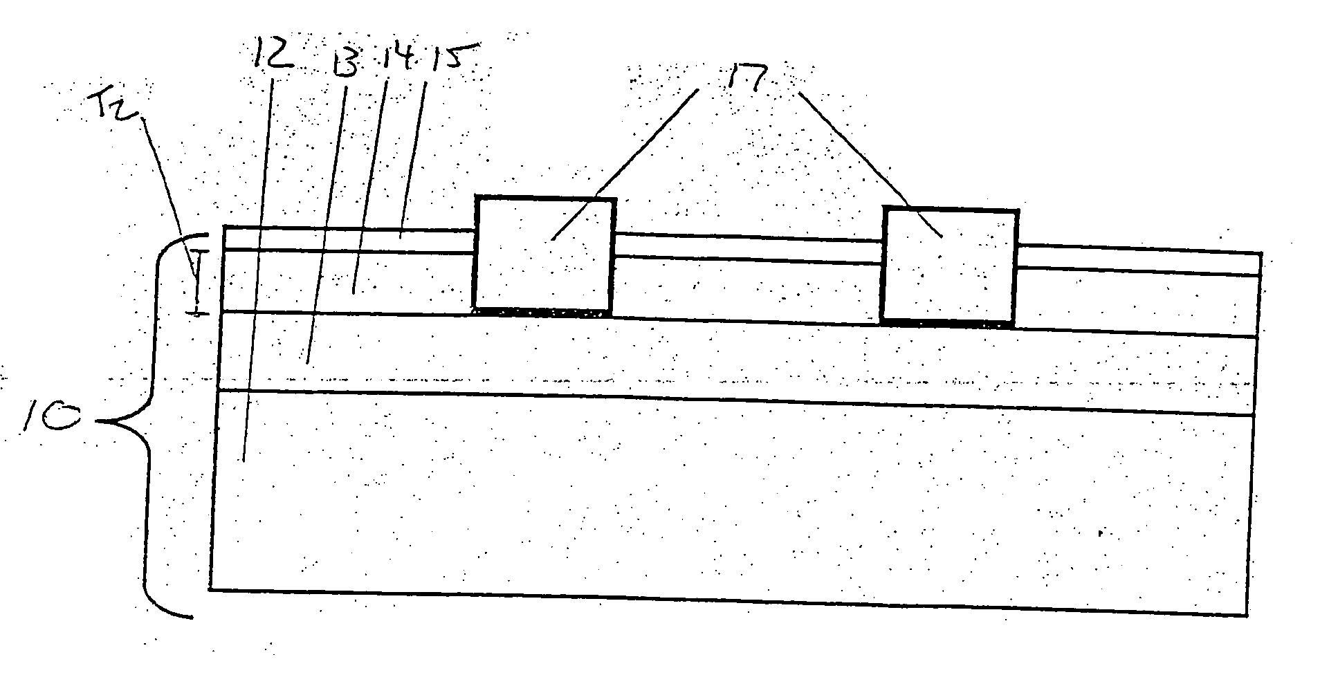
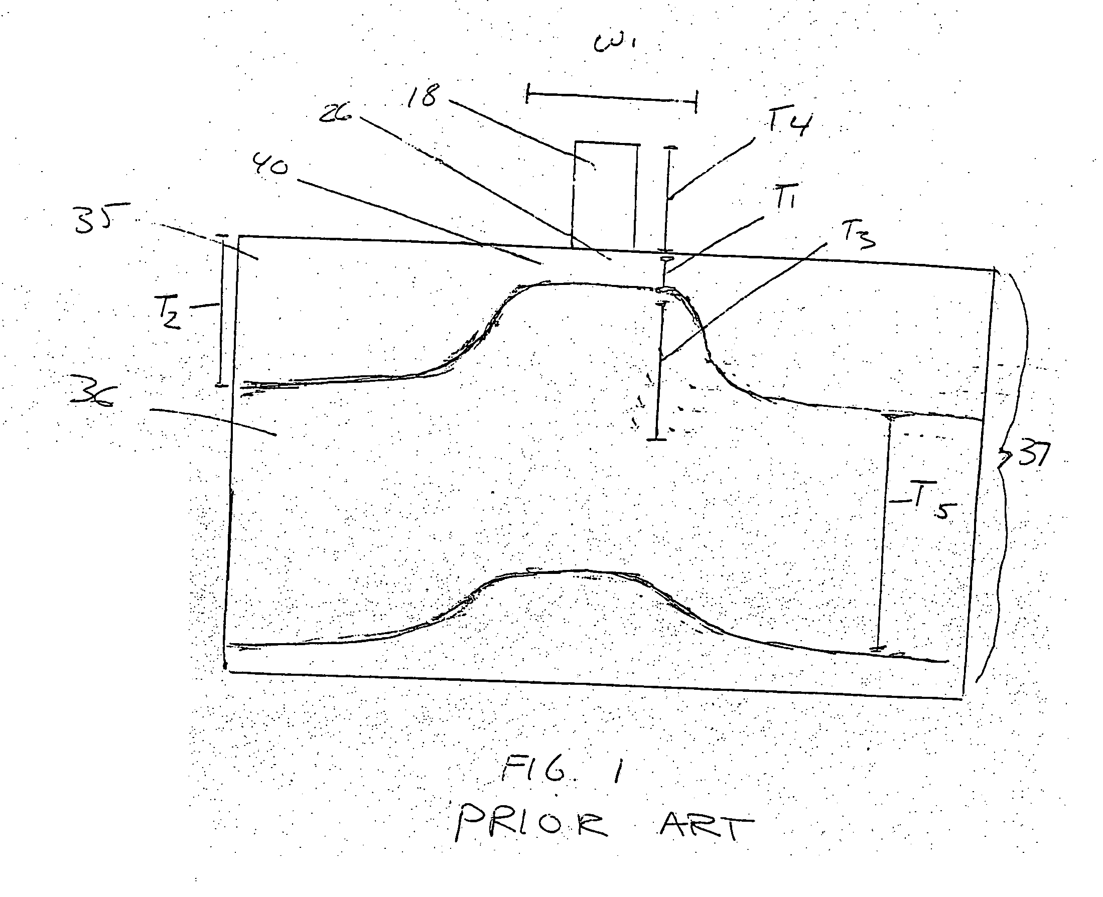
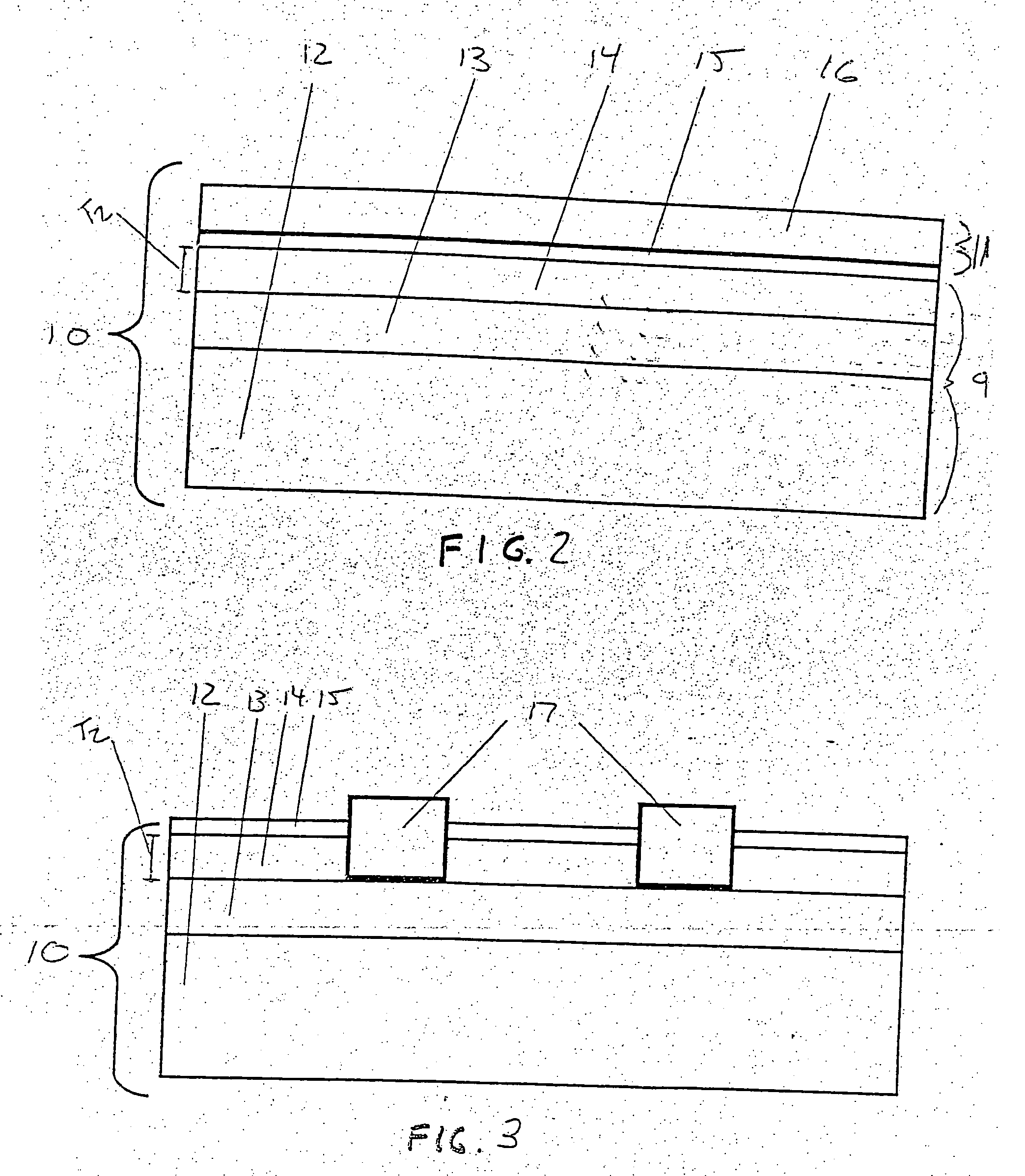
[0044] The present invention provides a method for forming an ultra-thin channel MOSFET having low resistance source / drain regions 24 formed in the SOI layer 14 of a silicon-on-insulator (SOI) substrate 9. The thickness T1 of the thin channel region 26 of the present invention is on the order of less than about 50.0 nm, preferably ranging from approximately 3.0 nm to approximately 30.0 nm.

[0045] The thin channel MOSFET produced by the inventive method further comprises a localized oxide region 25 self-aligned to an overlying gate region 23, where the localized oxide region 25 in conjunction with the buried insulating layer 13 of the SOI substrate 10 effectively thin the device channel 26. In addition to thinning the device channel, the localized oxide region 25 allows for the formation of source / drain extensions 24 within the SOI layer 14 having a thickness T2 sufficient to produce a low external resistance device. The present invention will now be described in more detail referrin...


PUM


Abstract

The present invention comprises a method for forming an ultra-thin channel MOSFET and the ultra-thin channel MOSFET produced therefrom. Specifically, the method comprises providing an SOI substrate having a buried insulating layer underlying an SOI layer; forming a pad stack atop the SOI layer; forming a block mask having a channel via atop the pad stack; providing a localized oxide region in the SOI layer on top of the buried insulating layer thereby thinning a portion of the SOI layer, the localized oxide region being self-aligned with the channel via; forming a gate in the channel via; removing at least the block mask; and forming source/drain extensions in the SOI layer abutting the thinned portion of the SOI layer. Providing the localized oxide region further comprises implanting oxygen dopant through the channel via into a portion of the SOI layer; and annealing the dopant to create the localized oxide region.

Description

FIELD OF INVENTION [0001] The present invention relates to semiconductor devices and methods of manufacture, and more particularly to a method for manufacturing an improved metal oxide semiconductor (MOS) transistor having an ultra-thin channel (on the order of about 50 nm or less). BACKGROUND OF THE INVENTION [0002] Field effect transistors (FETs) are the basic building block of today's integrated circuits (ICs). Such transistors can be formed in conventional bulk semiconductor substrates (such as silicon) or in the SOI layer of a silicon-on-insulator (SOI) substrate. [0003] In order to be able to make ICs, such as memory, logic, and other devices, of higher integration density than currently feasible, one has to find ways to further downscale the dimensions of field effect transistors (FETs), such as metal-oxide-semiconductor field effect transistors (MOSFETs) and complementary metal oxide semiconductors (CMOS). Scaling achieves compactness and improves operating performance in de...

Claims


Application Information

Patent Timeline
IPC IPC(8): H01L21/265H01L21/28H01L21/311H01L21/336H01L29/10H01L29/49H01L29/51H01L29/78
CPCH01L21/26533H01L21/28194H01L21/28202H01L29/1083H01L29/78H01L29/517H01L29/518H01L29/66545H01L29/49H01L21/2658
Inventor BOYD, DIANE C.DORIS, BRUCE B.IEONG, MEIKEISADANA, DEVENDRA K.
Owner GLOBALFOUNDRIES INC
Why Eureka
Try Eureka