Semiconductor device and a method of manufacturing the same

a technology of semiconductor devices and semiconductor chips, applied in the field of semiconductor devices, can solve the problems of reducing the number of ic chips to be mounted thereon, and reducing the size of ic chips, so as to increase the reliability of the driver circuit, reduce the frequency of the input digital signal, and reduce the tft of the stick driver

Inactive Publication Date: 2005-06-09
SEMICON ENERGY LAB CO LTD
View PDF16 Cites 36 Cited by
  • Summary
  • Abstract
  • Description
  • Claims
  • Application Information

AI Technical Summary

Benefits of technology

[0016] Further, means of lowering the frequency of a digital signal input to the stick driver is provided by forming a signal dividing circuit, formed in the data line side which requires a high frequency digital signal input. The load of the TFT of the stick driver is thus reduced, increasing the reliability of the driver circuit. The signal dividing circuit is provided with n input portions and m×n output portions, and by receiving the input signal from each of the n input portion, and by transmitting a corrected digital signal, in which the pulse length of the input digital signal is expanded in time, from the m×n output portions, thereby reducing the frequency of the input digital signal. The corrected digital signal may be expanded in time to several times the length of the input digital signal pulse.

Problems solved by technology

In such display devices, if the number of pixels increases, then the number of IC chips to be mounted thereon will also inevitably become large.
The size of the IC chip is limited by the wafer size in the manufacturing process, and the practical size limit of the longer side is on the order of 20 mm.
A method of manufacturing a long size IC chip has also been considered, but the number of strip shape IC chips which can be cut out from a circular shape silicon wafer is naturally lowered, and therefore the method is not practical.
In addition, the silicon wafer itself has a fragile nature, and if a rather long IC chip is manufactured, then the probability of breakage increases.
If the number of IC chips joined to one panel increases, then the probability of defects developing increases, which leads to a fear of reducing the yield in that process.
In addition, the temperature coefficient of the silicon which becomes the substrate of the IC chip differs from the temperature coefficient of the glass substrate on which the pixel region is formed, and therefore problems such as warping develop after the two substrates are joined.
This becomes a cause of a lowering in the reliability of the element due to the developed mechanical stress, as well as of direct defects such as an increase in the contact resistance.
However, if an area of surface of the circuit portion increases, the number of stick drivers which become defective due to a single point defect increases, and therefore the number which can be cut out of one substrate is reduced, causing a reduction in the process yield.

Method used


Image

  • Semiconductor device and a method of manufacturing the same
  • Semiconductor device and a method of manufacturing the same
  • Semiconductor device and a method of manufacturing the same

Examples


embodiment mode 1

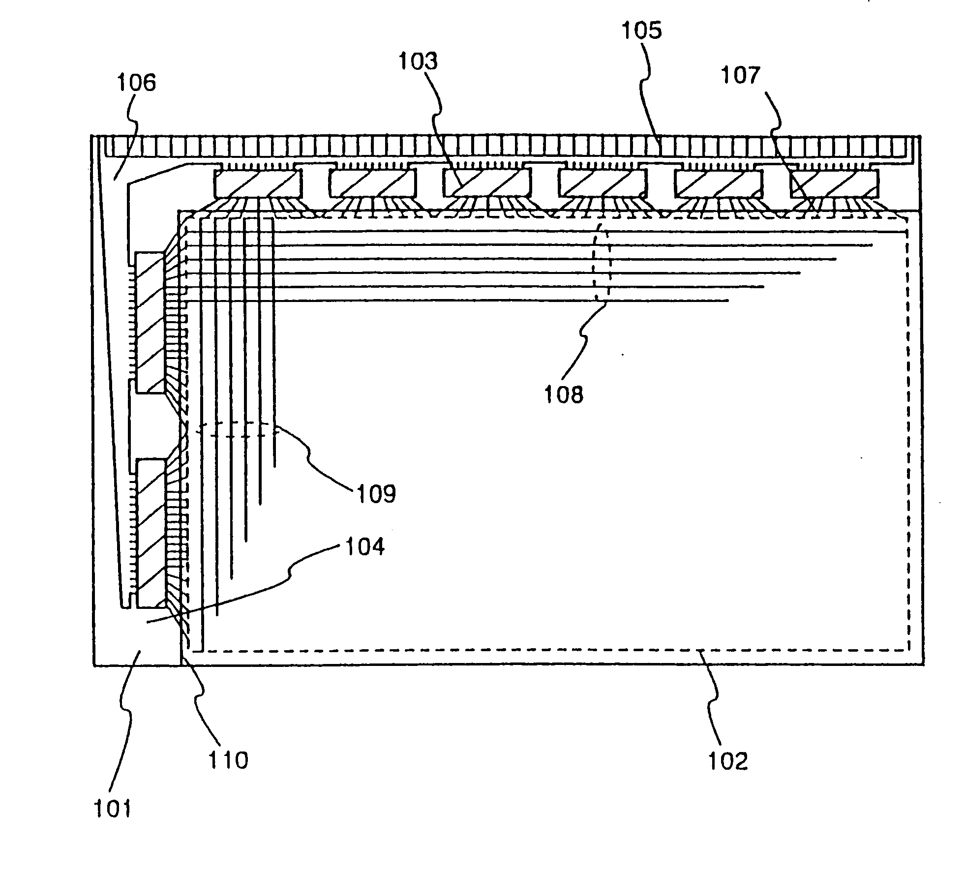
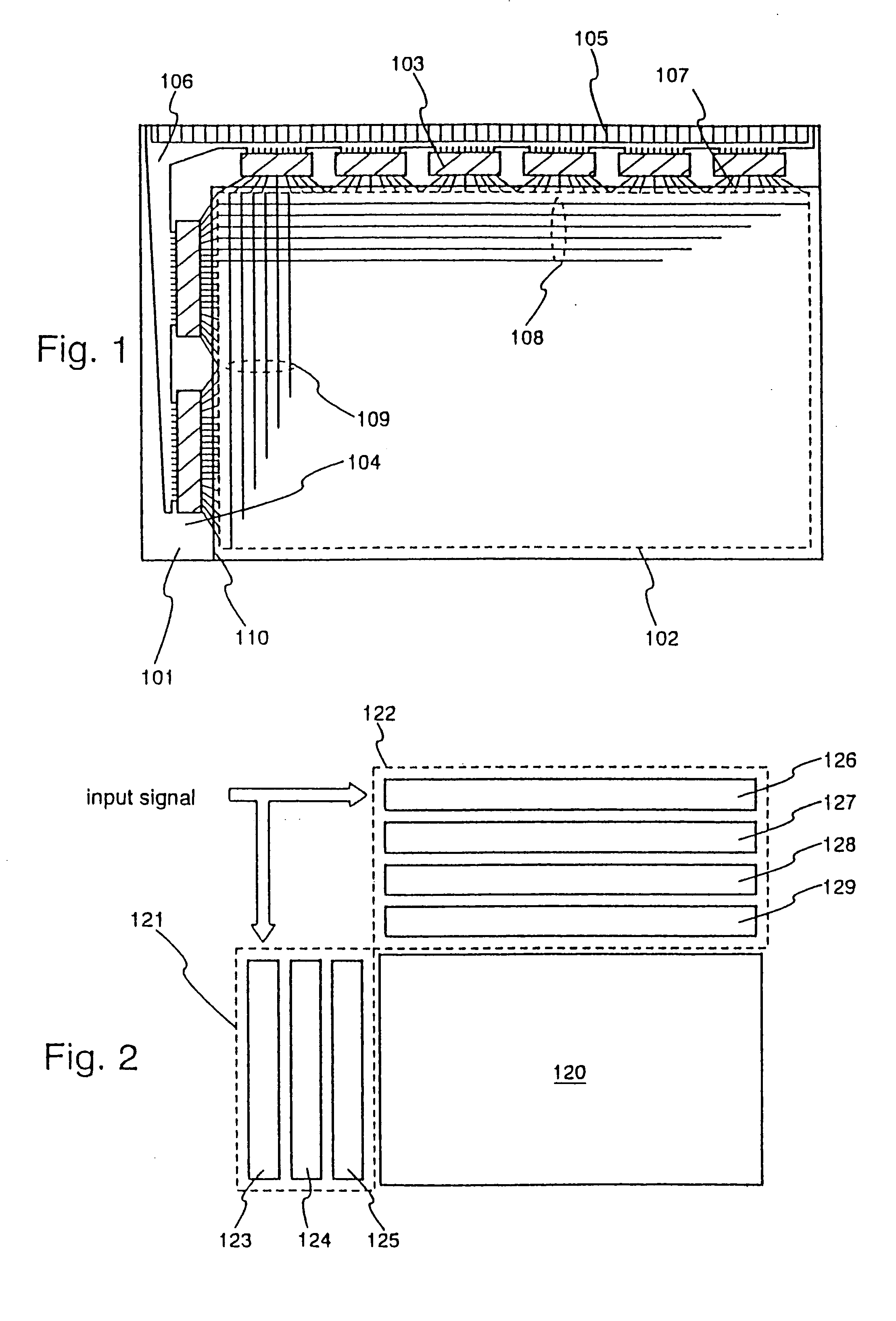
[0058]FIG. 1 is a diagram showing the structure of a display device of the present invention. A pixel region 102 is formed on a substrate 101. A second substrate 110, on which an opposing electrode is formed, is joined to the region in which the pixel region 102 has been formed, through a liquid crystal layer (not shown in the figure). The interval between the first substrate and the second substrate, namely the thickness of the liquid crystal layer, is determined by spacers, and is set from 3 to 8 μm for a nematic liquid crystal, and between 1 and 4 μm for a sumectic liquid crystal. It is preferable to use a non-alkaline glass such as aluminum borosilicate glass or barium borosilicate glass for the first substrate and the second substrate, and a thickness of 0.3 to 1.1 mm (typically 0.7 mm) is adopted, and therefore the thickness of the liquid crystal layer can be relatively ignored in outward appearance.

[0059] The pixel region 102 forms a matrix in which a scanning line (correspo...

embodiment mode 2

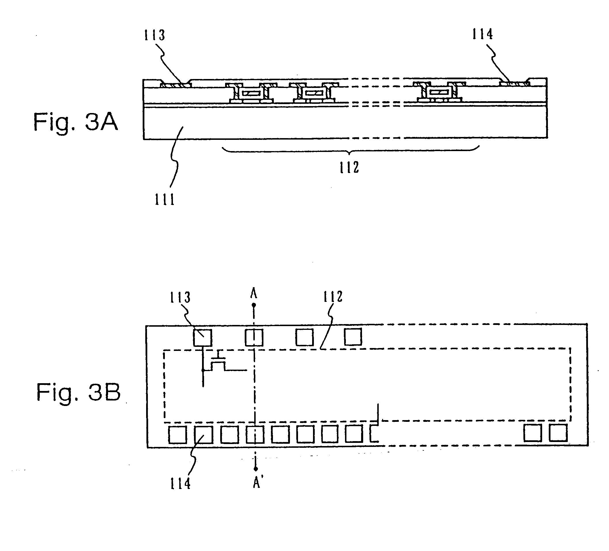
[0072] A method of manufacturing a TFT suitably applied mainly in a stick driver of a scanning line side is explained in this embodiment mode. Circuits such as a shift register circuit and a buffer circuit are formed in the stick driver on the scanning line side. The shift register circuit is assumed to be driven at 3 to 5 V, and the buffer circuit is assumed to be driven at 33 V. The TFT structuring the buffer circuit is required to have high voltage resistance, and therefore it is necessary for the film thickness of a gate insulating film to be thicker than that of other circuit TFTs. A manufacturing method thereof will be described with reference to FIGS. 6A to 6F and FIGS. 7A to 7E.

[0073] In FIG. 6A, a substrate such as a glass substrate, such as barium borosilicate glass or aluminum borosilicate glass, typically Corning Corp. #7059 or #1737, is used as a substrate 301. This type of glass substrate shrinks slightly due to the heating temperature, and if heat treatment processin...

embodiment mode 3

[0104] The voltage resistance required by a stick driver TFT formed on a data line side is on the order of 12 V, but the operating frequency is equal to or greater than 50 MHz (for example, 65 MHz) at 3 V. A method of manufacturing a TFT suitable for such is explained in this embodiment mode.

[0105] Material quality with which it is possible to realize a high electric field effect mobility and a low subthreshold coefficient (S value) is required in a crystalline semiconductor film forming a channel forming region of the TFT. In other words, the crystalline semiconductor film having characteristics in which a defect level becomes trap centered or recombination centered, and in which the grain boundary potential is low. FIGS. 8A to 8C show one example of a method of manufacturing such a crystalline semiconductor film.

[0106] A substrate able to withstand heat treatment at 600° C. (preferably 950° C.) and having an insulating surface can be applied as a substrate 401 in FIG. 8A. From t...


PUM

PropertyMeasurementUnit
lengthaaaaaaaaaa
lengthaaaaaaaaaa
sizeaaaaaaaaaa

Abstract

To form a driver circuit to be mounted to a liquid crystal display device or the like on a glass substrate, a quartz substrate, etc., and to provide a display device mounting driver circuits formed from different TFTs suited for their respective operational characteristics. A stick driver circuit on the scanning line side and a stick driver circuit on the data line side are different in structure, and have different TFTs in which the thickness of a gate insulating film, the channel length and other parameters are varied depending on required circuit characteristics. In the stick driver on the scanning line side, which is composed of a shift register circuit, a level shifter circuit, and a buffer circuit, the buffer circuit has a TFT with a thick gate insulating film because it is required to have a withstand voltage of 30 V. The stick driver circuit on the data line side, which is composed of a shift register circuit, a latch circuit, a level shifter circuit, and a D / A converter circuit, is driven at a high frequency, and hence its shift register circuit and latch circuit have thin gate insulating films and the channel length thereof is shorter than that of the TFT of the buffer circuit.

Description

BACKGROUND OF THE INVENTION [0001] 1. Field of the Invention [0002] The present invention relates to a semiconductor device having a display portion for displaying information such as images and characters. More particularly, the present invention relates to a structure of a driver circuit for transmitting a signal to each pixels in a pixel region that constitutes a display portion, to a method of manufacturing the same, and to amounting method thereof. Also, the present invention relates to a semiconductor device having a region in which thin film transistors are arranged in matrix, and in particular, to a circuit structure, its manufacturing method and its mounting method, which is formed separately with the above matrix circuit. Note that, throughout this specification, a semiconductor device denotes a general device that can function by utilizing semiconductor characteristics and that the category of semiconductor devices includes electronic equipment. [0003] 2. Description of t...

Claims


Application Information

Patent Timeline
Patent Type & Authority Applications(United States)
IPC IPC(8): G02F1/13H01L21/77H01L21/84H01L27/12H01L27/32H01L29/423H01L29/49H01L29/786
CPCG02F1/13452H01L27/1214H01L2224/45144H01L2224/73204H01L2224/48464H01L2224/48091H01L2224/32225H01L2224/16225H01L2029/7863H01L27/1237H01L27/3244H01L29/42384H01L29/4908H01L29/78621H01L29/78627H01L29/78696H01L2924/00014H01L2924/00H01L2224/05573H01L2224/05568H10K59/12
Inventor YAMAZAKI, SHUNPEIKOYAMA, JUNARAI, YASUYUKI
Owner SEMICON ENERGY LAB CO LTD
Why Eureka
Try Eureka