Methods of forming oxide masks with submicron openings and microstructures formed thereby

a technology of oxide masks and openings, applied in the manufacture of microstructural devices, microstructures, electrical equipment, etc., can solve the problem of the selectiveness of the etching process to the mask material, and achieve the effects of high quality factor, reliability and long-term thermal stability, and high processing yield

Active Publication Date: 2005-06-09
GEORGIA TECH RES CORP
View PDF17 Cites 115 Cited by
  • Summary
  • Abstract
  • Description
  • Claims
  • Application Information

AI Technical Summary

Benefits of technology

[0012] One of the major applications the present invention is fabrication of fully single crystal silicon (SCS) capacitive resonators or sensors with deep-submicron capacitive transducer gaps (i.e., high aspect-ratio trenches) and high quality factor (Q). Using the present invention, since these structures and their electrodes can be made from single crystal silicon, much higher processing yield, reliability and long-term thermal stability can be achieved compared to resonators made using a combination of SCS and metal or polysilicon. The present invention provides for this using commercially available materials and processes. Therefore integration of high quality factor resonators and filters with existing CMOS electronics is possible.

Problems solved by technology

A great challenge in extending the frequency of capacitive micromechanical resonators into the RF range is maintaining acceptable impedance level and power handling capability.
However, there are some challenges.
The other limiting factor is the selectivity of the etching process to the mask material.

Method used


Image

  • Methods of forming oxide masks with submicron openings and microstructures formed thereby
  • Methods of forming oxide masks with submicron openings and microstructures formed thereby
  • Methods of forming oxide masks with submicron openings and microstructures formed thereby

Examples


Embodiment Construction

[0031] The present invention provides for microstructures and fabrication methods wherein, preferably, a single mask, and conventional photolithographic techniques are used to produce the microstructures. Various types of microstructures may be produced. In its most basic form, the present invention provides for methods of processing a substrate to form an oxide mask thereon having submicron openings.

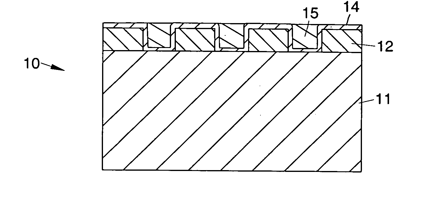
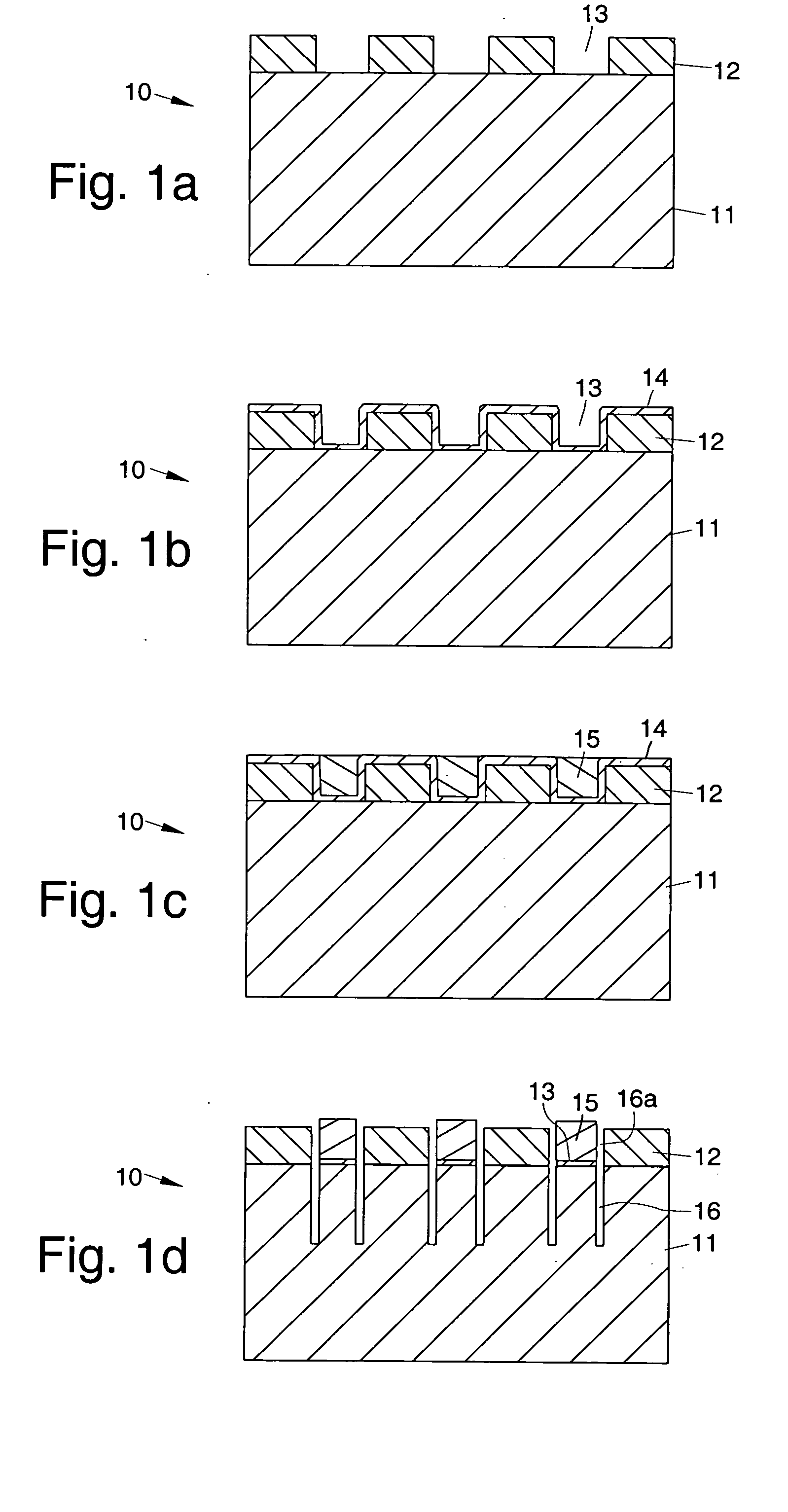
[0032] Referring to the drawing figures, FIGS. 1a-1d schematically illustrate processing steps of an exemplary method 10 in accordance with the present invention used to form submicron openings 16a in an oxide mask. In the exemplary method 10, a layer of oxide 12 is formed on a substrate 11 (FIG. 1a). The layer of oxide 12 is patterned to form shallow trenches 13 therein (FIG. 1a). A layer of sacrificial polysilicon 14 is deposited on the patterned layer of oxide 12 (FIG. 1b). A second layer of oxide 15 is deposited on the patterned layer of sacrificial polysilicon 14 and is etched bac...


PUM

PropertyMeasurementUnit
thickaaaaaaaaaa
aspect ratioaaaaaaaaaa
thickaaaaaaaaaa

Abstract

Processing techniques are disclosed for batch fabrication of microstructures comprising an oxide mask on a substrate with submicron openings formed therein, and microstructures having deep-submicron, high aspect-ratio etched trenches, using conventional optical photolithography. Exemplary high aspect-ratio etched-trench microstructures that may be produced include single crystal resonators and sensors.

Description

GOVERNMENT RIGHTS [0001] The U.S. Government has a paid-up license in this invention and the right in limited circumstances to require the patent owner to license others on reasonable terms as provided for by the terms of DAAH01-01-1-R004 awarded by DARPA of the U.S. Government.BACKGROUND [0002] The present invention relates generally to semiconductor microstructures and fabrication methods, and more particularly, to methods of forming oxide masks on substrates that have submicron openings therein and which are formed using conventional optolithography techniques, and microstructures formed using the methods, including microstructures having high aspect ratio submicron trenches formed therein. [0003] Deep-sub-micron vertical gaps are required in certain MEMS devices to increase the capacitive electromechanical coupling. Higher coupling results in higher signal to noise ratio in sensors and lower equivalent motional impedance in electromechanical resonators. [0004] High Q integrated ...

Claims


Application Information

Patent Timeline
Patent Type & Authority Applications(United States)
IPC IPC(8): H01L21/00H01L21/76
CPCB81C1/00619
Inventor AYAZI, FARROKHABDOLVAND, REZAANARAKI, SIAVASH P.
Owner GEORGIA TECH RES CORP
Why Eureka
Try Eureka