

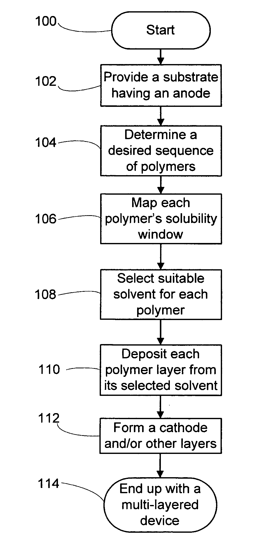
Multi-layered device and method for making the same
a multi-layer device and film technology, applied in the field of electro-optic devices, can solve the problems of difficult to achieve continuous and coalesced film coverage, difficult to meet the various demands of opto-electronic applications, and the preparation of multiple polymer layers is problematic, etc., to achieve good adhesion, improve brightness, life and efficiency
- Summary
- Abstract
- Description
- Claims
- Application Information
AI Technical Summary
Benefits of technology
Problems solved by technology
Method used
Image

Examples
example 1
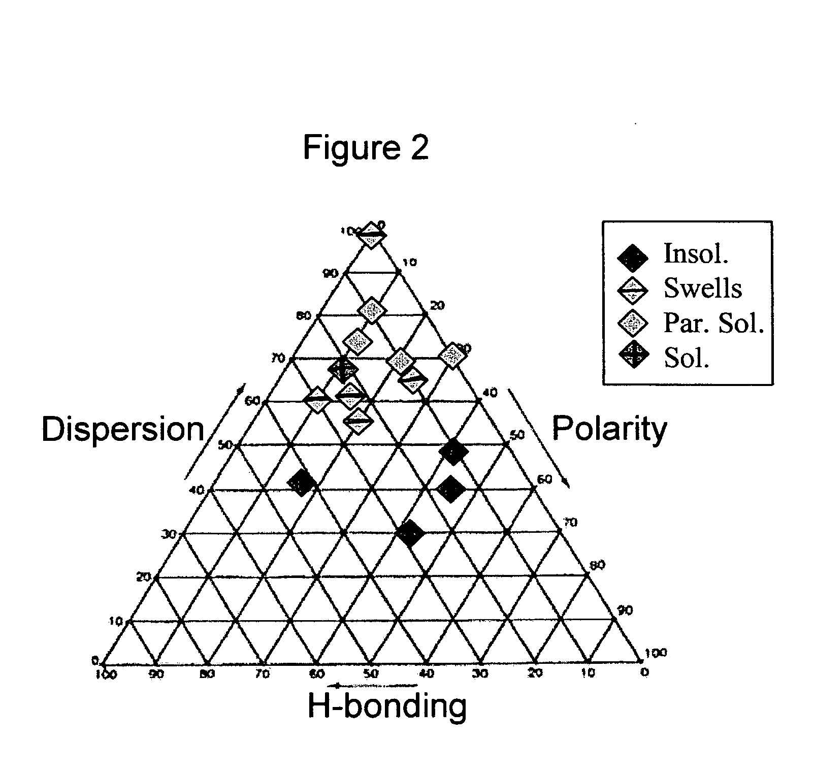
[0033]FIG. 2 illustrates a solubility graph for a first blue emissive polyfluorene (BEPF1) according to an exemplary embodiment of the invention. Solubility observations (soluble, partially soluble, swelling and insoluble) were based on experiments incorporating 5% solids at room temperature (22° C.) for the BEPF1. The data were plotted in the Teas graph as shown in FIG. 2, wherein the graph points are different solvents as defined by their fractional solubility parameters. The color code denotes the observation of relative solubility. A solubility window for a polymer is described by the region where the polymer exhibits solubility or partial solubility. The solubility window for the BEPF1 was roughly identified by 65dphd, fp and fh represent the fractional contribution of dispersion force, polarity force and hydrogen-bonding force, respectively, to the overall Hildebrand parameter of a solvent.
[0034]FIG. 3 illustrates a solubility graph for another polymer according to an exempla...
example 2
[0037]FIG. 5 illustrates a cross-sectional view of a multi-layered polymer light emitting device according to an exemplary embodiment of the invention.
[0038] A polymer light emitting device (PLED) was successfully fabricated utilizing the multi-layer approach described above. Two polymer layers were sequentially spun cast from solution to create a bi-layer, solution-processed PLED. An indium-tin-oxide (ITO) 502 coated glass substrate 500 was cleaned using solvents. Upon further ultraviolet ozone treatment, PEDOT was spun onto the substrate at 5000 RPM to form a PEDOT layer 504 approximately 700 Å thick. After baking the substrate at 170° C. for one hour, an emissive polymer layer 506 comprising a second blue emissive polyfluorine (BEPF2) approximately 700 Å thick was spun on. This was followed by an approximately 200Å-thick KL-22 (a polymethylmethacrylate co-polymer containing 1% Polyfluor™ 394 available from Polysciences, Inc.) layer 508, a resistive energy transport layer, spun c...
example 3
[0039]FIG. 6 illustrates a solubility graph for a third blue emissive polyfluorine (BEPF3) according to an exemplary embodiment of the invention. Solubility observations (soluble, partially soluble, swells, insoluble) were based on experiments incorporating 10% solids at room temperature (22° C.) for the BEPF3. The data were plotted according to the Teas method.
[0040] As can be seen, a boundary region exists at about fd=60. Below that value swelling and insolubility are noted. The region closest to the solubility boundary should prove to be a region of strong attraction and therefore high adhesion. This region is best described by the coordinates: 45dphd>60) or poor adhesion (fd<45). It is further noteworthy that the location of the boundary region is expected to be temperature dependent (high temperatures lower the boundary, lower temperatures raise it).
[0041] A pinhole free film of the BEPF3 was deposited onto a glass slide from a 10% cumene solution measuring 1.65 μm in thickne...
PUM
| Property | Measurement | Unit |
|---|---|---|
| thick | aaaaa | aaaaa |
| temperature | aaaaa | aaaaa |
| operating voltage | aaaaa | aaaaa |
Abstract
Description
Claims
Application Information