Semiconductor device and method for manufacturing semiconductor device

a semiconductor layer and semiconductor technology, applied in the direction of semiconductor devices, basic electric elements, electrical appliances, etc., can solve the problems of deterioration of high frequency characteristics or so-called frequency dispersion, insufficient suppression of frequency dispersion, and difficulty in forming a minute concave portion in the upper portion of the iii-v nitride semiconductor layer, etc., to reduce the influence of traps, suppress frequency dispersion, and the effect of gate length

Inactive Publication Date: 2005-06-30
PANASONIC CORP
View PDF4 Cites 59 Cited by
  • Summary
  • Abstract
  • Description
  • Claims
  • Application Information

AI Technical Summary

Benefits of technology

[0018] Specifically, according to a first aspect of the present invention, there is provided a semiconductor device, comprising: a III-V nitride semiconductor layer including a channel region in which carriers travel; a concave portion provided in an upper portion of the channel region in the III-V nitride semiconductor layer; and a Schottky electrode consisting of a conductive material forming a Schottky junction with the semiconductor layer, and formed on a semiconductor layer, which spreads over the concave portion and peripheral portions of the concave portion, on the III-V nitride semiconductor layer, wherein a dimension of the concave portion in a depth direction is set so that a portion of the Schottky electrode provided in the concave portion can adjust a quantity of the carriers traveling in the channel region.
[0019] In the semiconductor device of the...

Problems solved by technology

Nevertheless, because of presence of a high density trap level on a surface of the III-V nitride semiconductor, carries are captured and emitted in traps on the surface of the AlGaN layer, with the result that a phenomenon of deterioration in high frequency characteristics or so-called frequency dispersion occurs.
However, in a fringe region that is a lower side end of the gate electrode, surface charge influences the channel region, with the result that the frequency dispersion cannot be sufficiently suppressed.
However, if the spike-gate structure of the con...

Method used


Image

  • Semiconductor device and method for manufacturing semiconductor device
  • Semiconductor device and method for manufacturing semiconductor device
  • Semiconductor device and method for manufacturing semiconductor device

Examples


embodiment 1

[0068] A III-V nitride semiconductor device in the first embodiment of the present invention will be described with reference to the drawings. In the present specification, the III-V nitride semiconductor is a hybrid semiconductor including one of or two or more of boron nitride (BN), aluminum nitride (AlN), gallium nitride (GaN), and indium nitride (InN), and represented by a general formula of BxAlyGazIn1-x-yN (where 0≦x≦1, 0≦y≦1, and ≦0z≦z≦1).

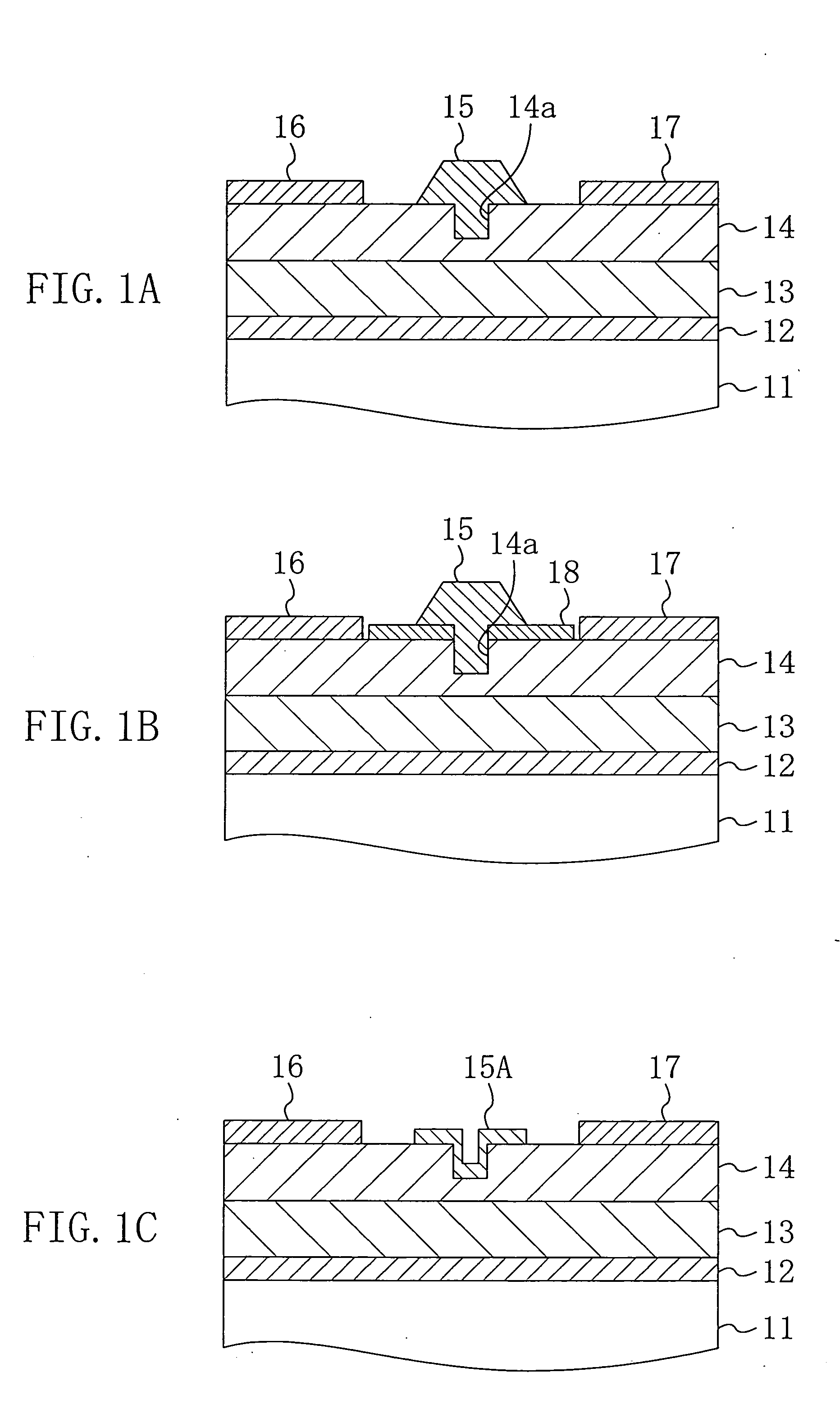
[0069]FIG. 1A is a cross-sectional block diagram of the III-V nitride semiconductor device in the first embodiment of the present invention. As shown in FIG. 1A, the III-V nitride semiconductor device is constituted so that, for example, a buffer layer 12 having a thickness of about 10 nm to 200 nm and consisting of aluminum nitride (AlN), a channel layer 13 having a thickness of about 2 μm to 3 μm and consisting of undoped gallium nitride (GaN), and a carrier supply layer 14 having a thickness of about 20 nm to 30 nm and consisting of n ty...

modification 1

of Embodiment 1

[0077]FIG. 1B is a cross-sectional block diagram of a III-V nitride semiconductor device in the first modification of the first embodiment of the present invention. As shown in FIG. 1B, the III-V nitride semiconductor device in the first modification is constituted so that a protection film 18 having a thickness of about 100 nm to 200 nm and consisting of silicon oxide or silicon nitride is provided in a region between the concave portion 14a and each of the source electrode 16 and the drain electrode 17 on the upper surface of the carrier supply layer 14.

[0078] According to the first modification of the first embodiment, since the protection film 18 is provided on the upper surface of the carrier supply layer 14, a trap density in both side portions of the gate electrode 15 on the upper surface of the carrier supply layer 14 can be reduced. It is, therefore, possible to further ensure suppressing the frequency dispersion resulting from the traps on the upper surface...

modification 2

of Embodiment 1

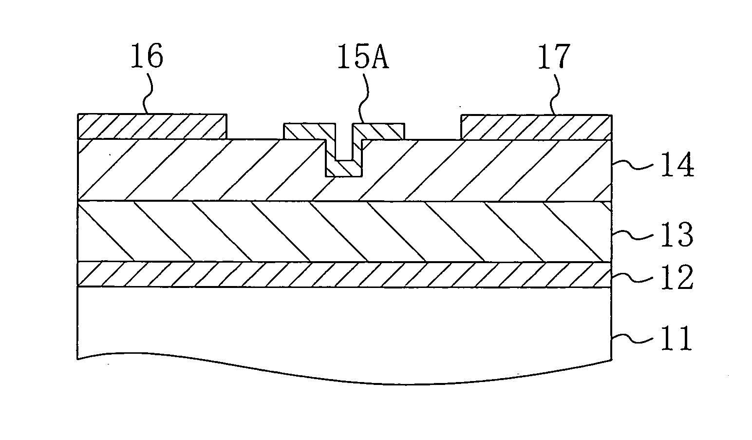
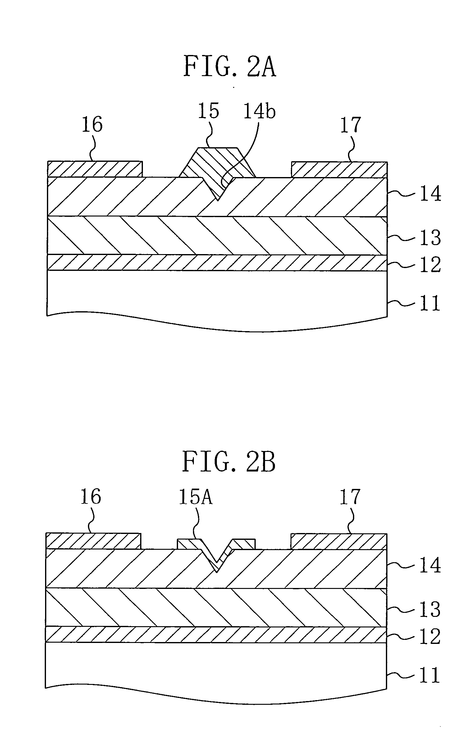
[0080]FIG. 1C is a cross-sectional block diagram of a III-V nitride semiconductor device in the second modification of the first embodiment of the present invention. As shown in FIG. 1C, the III-V nitride semiconductor device in the second modification is constituted so that a gate electrode 15A formed in the concave portion 14a, which is provided on the upper surface of the carrier supply layer 14, and serving as a Schottky electrode is provided not to be filled into the concave portion 14a but to extend along a bottom and a wall surface of the concave portion 14a and peripheral portions of the concave portion 14a. Since the gate electrode 15A is not filled into the concave portion 14a, an amount of a material used for the gate electrode 15A can be reduced and a throughput of a step of forming the gate electrode 15A can be improved.

Embodiment 2

[0081] A III-V nitride semiconductor device in the second embodiment of the present invention will be described hereinafter...


PUM


Abstract

A semiconductor device of the present invention includes: a III-V nitride semiconductor layer including a channel region in which carriers travel; a concave portion provided in an upper portion of the channel region in the III-V nitride semiconductor layer; and a Schottky electrode consisting of a conductive material forming a Schottky junction with the semiconductor layer, and formed on a semiconductor layer, which spreads over the concave portion and peripheral portions of the concave portion, on the III-V nitride semiconductor layer. A dimension of the concave portion in a depth direction is set so that a portion of the Schottky electrode provided in the concave portion can adjust a quantity of the carriers traveling in the channel region.

Description

CROSS-REFERENCE TO RELATED APPLICATIONS [0001] All the matters disclosed in the claims, the specification, and the drawings of Japanese Patent Application No. 2003-432886 filed on Dec. 26, 2003 are incorporated herein by reference. BACKGROUND OF THE INVENTION [0002] The present invention relates to a semiconductor device using a III-V nitride semiconductor and a method for manufacturing the semiconductor device. More specifically, the present invention relates to a semiconductor device having a Schottky electrode formed on a semiconductor layer consisting of a III-V nitride semiconductor, and a method for manufacturing the semiconductor device. [0003] Conventionally, a III-V nitride semiconductor such as gallium nitride (GaN) has been widely used as a material for an active layer of an optical device since it has a direct transition energy band structure and a wide band gap. Recently, since the III-V nitride semiconductor is characteristically high in breakdown field intensity and h...

Claims


Application Information

Patent Timeline
IPC IPC(8): H01L21/28H01L21/335H01L21/338H01L29/20H01L29/423H01L29/778H01L29/812
CPCH01L21/28H01L29/2003H01L29/42316H01L29/8128H01L29/66871H01L29/7787H01L29/66462
Inventor MURATA, TOMOHIROHIROSE, YUTAKATANAKA, TSUYOSHIUEMOTO, YASUHIRO
Owner PANASONIC CORP
Why Eureka
Try Eureka