Transistor with silicon and carbon layer in the channel region

a technology of silicon and carbon layer, applied in the direction of semiconductor devices, transistors, electrical apparatus, etc., can solve the problems of reducing the speed and performance of transistors having high k gate dielectric materials, affecting and affecting the use of thin oxides in many device applications, so as to improve the electrical performance of transistors and electrical parameters, improve the electron and hole mobility, and increase the speed

Inactive Publication Date: 2005-06-30
INFINEON TECH AG
View PDF12 Cites 54 Cited by
  • Summary
  • Abstract
  • Description
  • Claims
  • Application Information

AI Technical Summary

Benefits of technology

[0007] These and other problems are generally solved or circumvented, and technical advantages are generally achieved, by preferred embodiments of the present invention which comprise a MOS device having a stressed channel, which increases the speed of the MOS device and improves the device performance. A layer of silicon and carbon is epitaxially grown in a channel region of the MOS device. The layer of silicon and carbon may be disposed over an optional epitaxially grown stressed semiconductor layer. An optional thin semiconductor material may be deposited over the layer of silicon and carbon. The layer of silicon and carbon and optional stressed semiconductor layer create a stressed region in the channel of the MOS device, which is advantageous because the electron mobility and hole mobility are improved. The stressed semiconductor layer lowers the interface of the lattice mismatch between the underlying workpiece and the layer of silicon and carbon, which further improves the performance of the MOS device.
[0012] Advantages of preferred embodiments of the present invention include providing a transistor design and manufacturing method thereof wherein the electrical performance of the transistor and electrical parameters are improved. The transistor has increased speed and may be manufactured in smaller dimensions. Epitaxially grown material layers are introduced into the channel region to introduce stress in the crystalline structure, improving the electron and hole mobility. The drive current of the transistor is also increased.

Problems solved by technology

However, as devices are scaled down in size, silicon dioxide becomes a problem because of gate leakage current, which can degrade device performance.
For low power logic (for portable electronic applications, for example), the main issue is low leakage current, which is absolutely necessary in order to extend battery life.
However, the resulting gate leakage currents make the use of such thin oxides impractical in many device applications where low standby power consumption is required.
However, the device performance of using high k dielectric materials suffers from trapped charge in the dielectric layer which deteriorates the mobility, making the drive current lower than in transistors having silicon dioxide gate oxides, and hence reducing the speed and performance of transistors having high k gate dielectric materials.

Method used


Image

  • Transistor with silicon and carbon layer in the channel region
  • Transistor with silicon and carbon layer in the channel region
  • Transistor with silicon and carbon layer in the channel region

Examples


Embodiment Construction

[0021] The making and using of the presently preferred embodiments are discussed in detail below. It should be appreciated, however, that the present invention provides many applicable inventive concepts that can be embodied in a wide variety of specific contexts. The specific embodiments discussed are merely illustrative of specific ways to make and use the invention, and do not limit the scope of the invention.

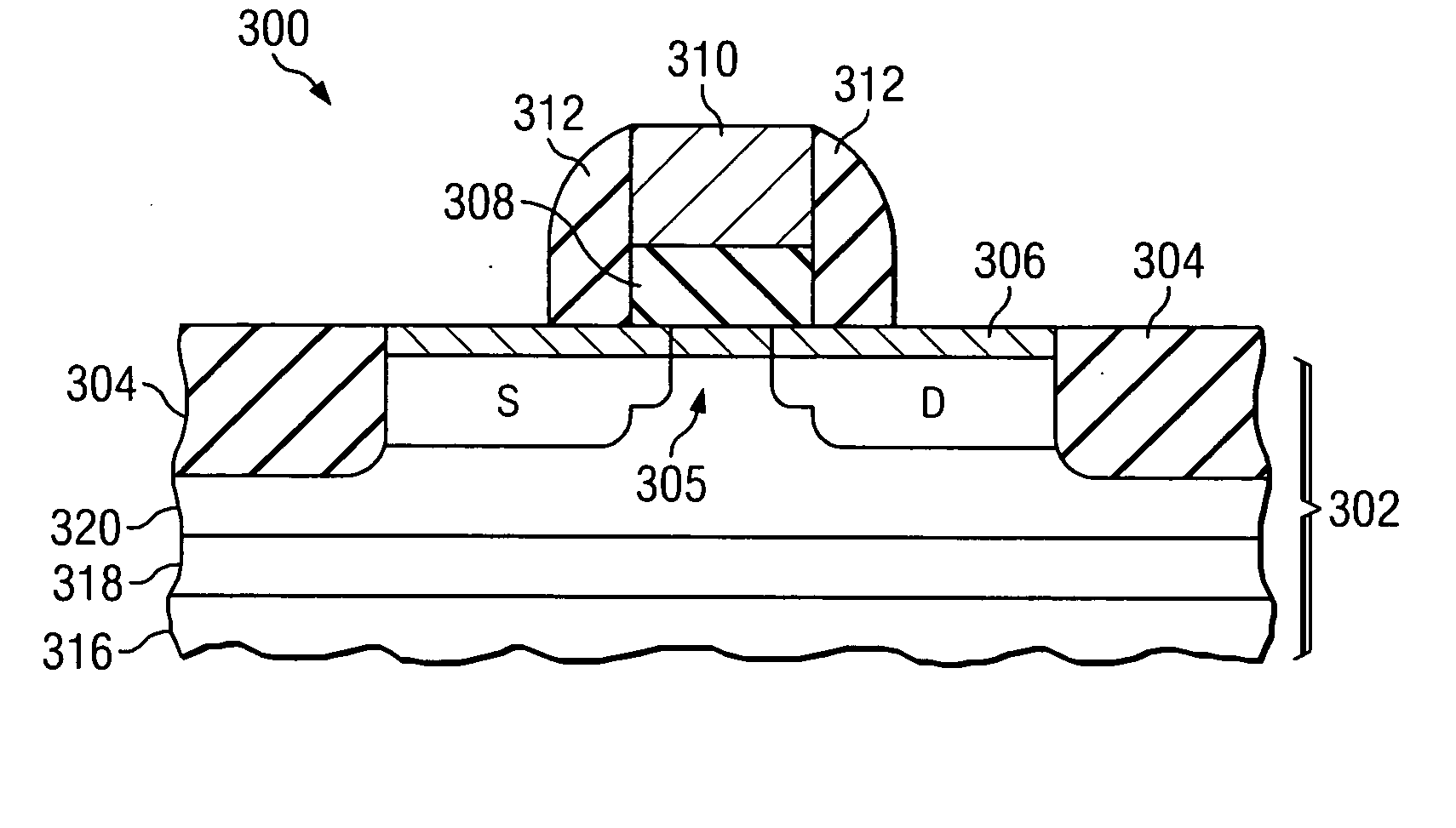
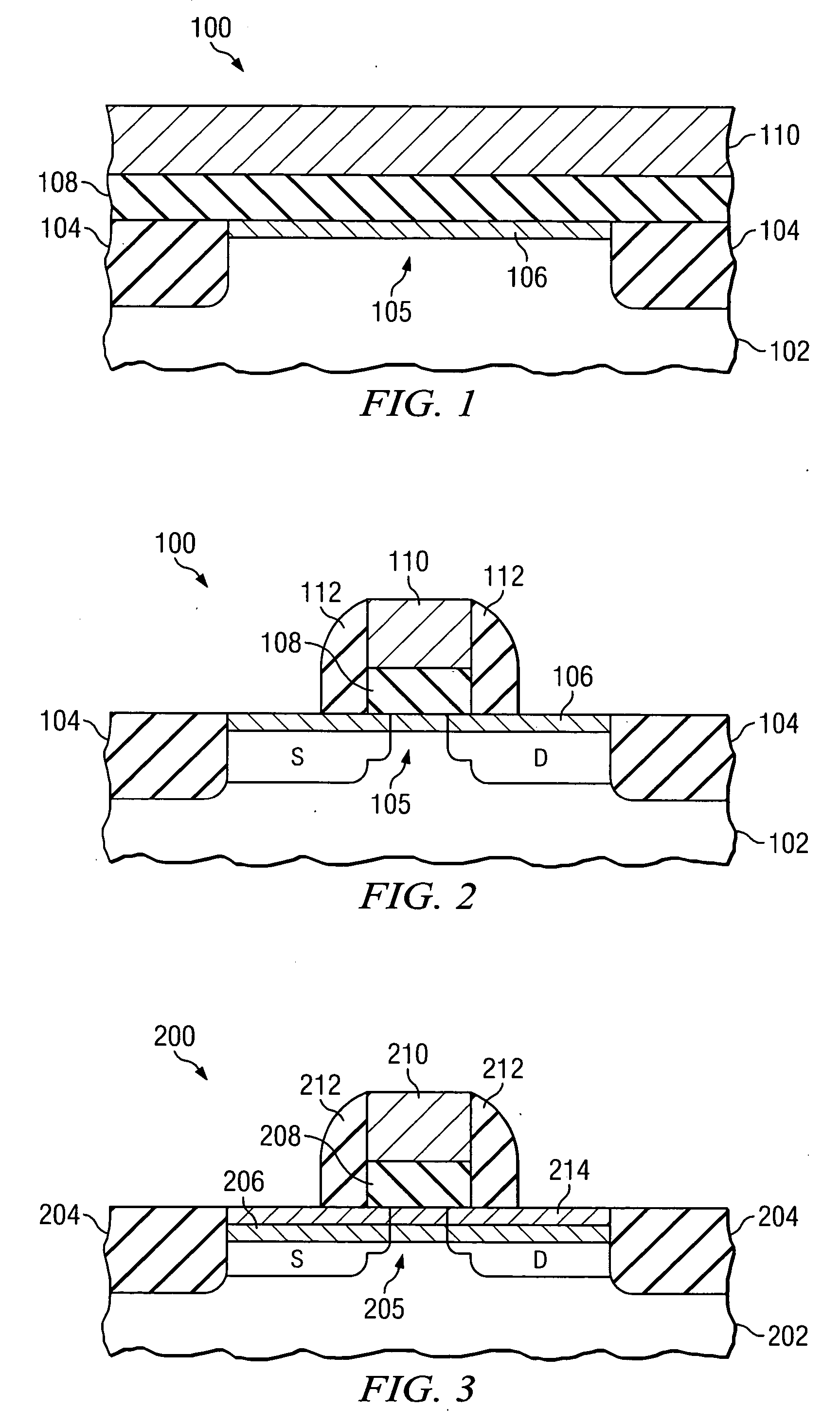
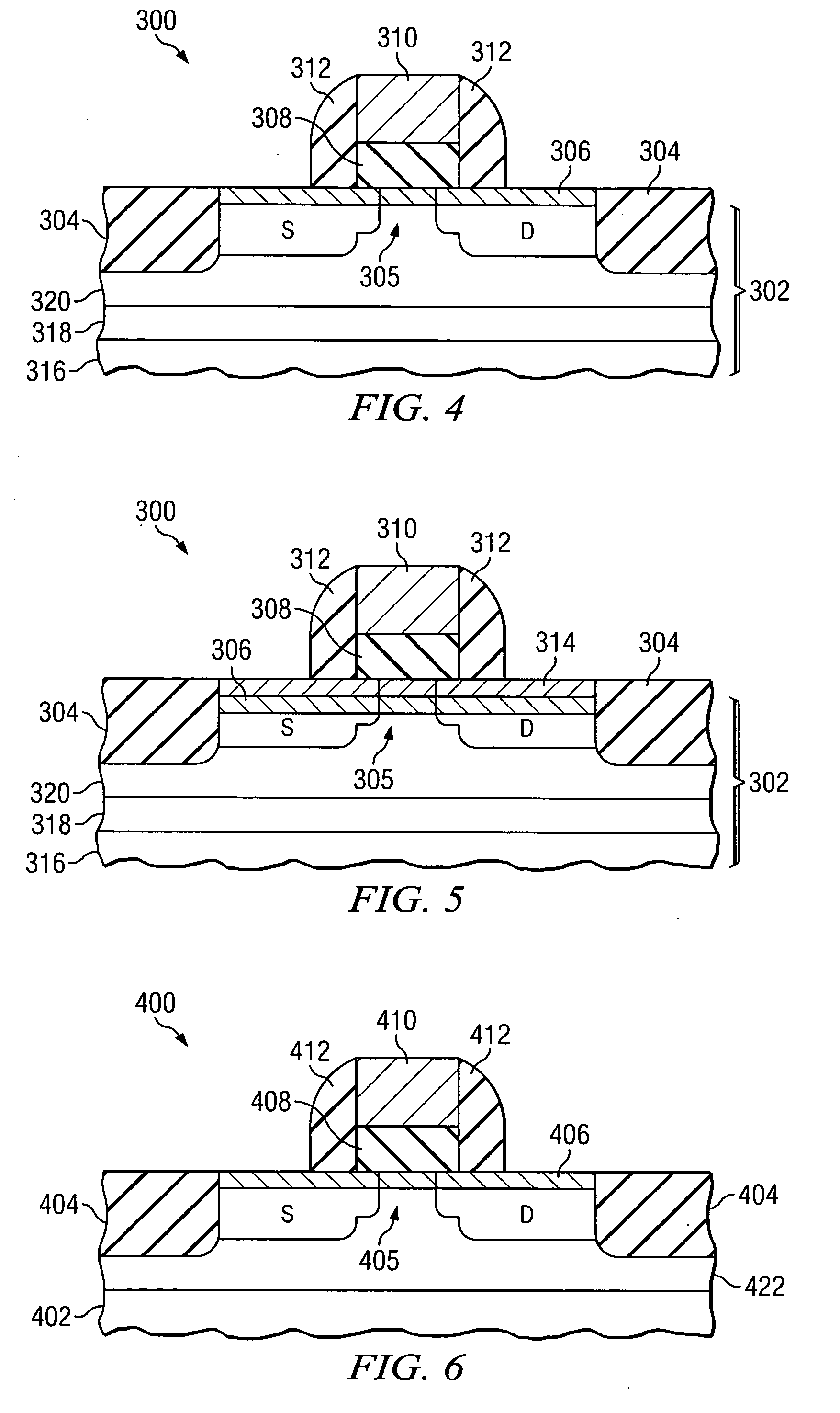
[0022] The present invention will be described with respect to preferred embodiments in a specific context, namely a transistor formed on a semiconductor device. The invention may also be applied, however, to MOSFETs, or other transistor devices, and may include PMOS, NMOS, or CMOS devices, as examples. Only one transistor is shown in each of the figures; however, there may be many transistors formed on the semiconductor devices shown.

[0023]FIGS. 1 and 2 show cross-sectional views of a transistor at various stages of manufacturing in accordance with a preferred embodiment ...


PUM

PropertyMeasurementUnit
thicknessaaaaaaaaaa
thicknessaaaaaaaaaa
thicknessaaaaaaaaaa

Abstract

A transistor and method of manufacturing thereof having stressed material layers formed in the channel to increase the speed and improve performance of the transistor. A layer of silicon and carbon is epitaxially grown in the channel region. A thin semiconductor material may be formed over the layer of silicon and carbon, and a stressed semiconductor layer may be epitaxially grown prior to forming the layer of silicon and carbon.

Description

TECHNICAL FIELD [0001] The present invention relates generally to semiconductor devices, and more particularly to a method of fabricating a transistor and a structure thereof. BACKGROUND [0002] Semiconductor devices are used in a variety of electronic applications, such as personal computers, cell phones, digital cameras, and other electronic equipment, as examples. A transistor is an element that is utilized extensively in semiconductor devices. There may be millions of transistors on a single integrated circuit (IC), for example. A common type of transistor used in semiconductor device fabrication is a metal oxide semiconductor field effect transistor (MOSFET). [0003] The gate dielectric for MOSFET devices has in the past typically comprised silicon dioxide. However, as devices are scaled down in size, silicon dioxide becomes a problem because of gate leakage current, which can degrade device performance. Therefore, there is a trend in the industry towards the development of the u...

Claims


Application Information

Patent Timeline
Patent Type & Authority Applications(United States)
IPC IPC(8): H01L21/04H01L21/28H01L29/10H01L29/49H01L29/51
CPCH01L21/28194H01L29/1054H01L29/66068H01L29/517H01L29/495
Inventor LI, HONG-JYH
Owner INFINEON TECH AG
Why Eureka
Try Eureka