High-frequency module and its manufacturing method

a technology of high-frequency modules and manufacturing methods, applied in the direction of high-frequency circuit adaptations, printed circuit non-printed electric components association, waveguide type devices, etc., can solve the problems of difficult to make a sufficient gain, communication terminals cannot be designed compact and lightweight, easy to be done, etc., to improve the performance and reliability of high-frequency modules, improve precision, and reduce costs

Inactive Publication Date: 2005-07-07
SONY CORP
View PDF9 Cites 44 Cited by
  • Summary
  • Abstract
  • Description
  • Claims
  • Application Information

AI Technical Summary

Benefits of technology

[0036] The above method of producing a high-frequency module according to the present invention permits to produce a high-frequency module with a reduced cost since the organic substrate is available at a relatively low price, and the conductive parts forming the passive elements and distributed parameter elements can be formed with an improved precision since the elements block is formed on the flat buildup surface of

Problems solved by technology

However, the above data communications can be done easily, not via any repeater or the like.
However, since each of the filters interposed between the stages cannot be assembled in any IC, the matching circuit has to be provided as an external device for the high-frequency transmission/reception circuit.
Therefore, the high-frequency transmission/reception circuit as a whole is so large that the communication terminal cannot be designed compact and lightweight.
In the high-frequency transmission/reception circuit, since signals are amplified once in the high-frequency stage, so it is difficult to make a sufficient gain.
Therefore, a DC offset cancel circuit and an extra lowpass filter have to be provided in the high-frequency transmission/reception circuit, which will lead to a larger total power consumption.
The conventional high-frequency transmission/reception circuit, whether of the aforementioned superheterodyne type or of the direct conversion type, does not meet the r

Method used


Image

  • High-frequency module and its manufacturing method
  • High-frequency module and its manufacturing method
  • High-frequency module and its manufacturing method

Examples


second embodiment

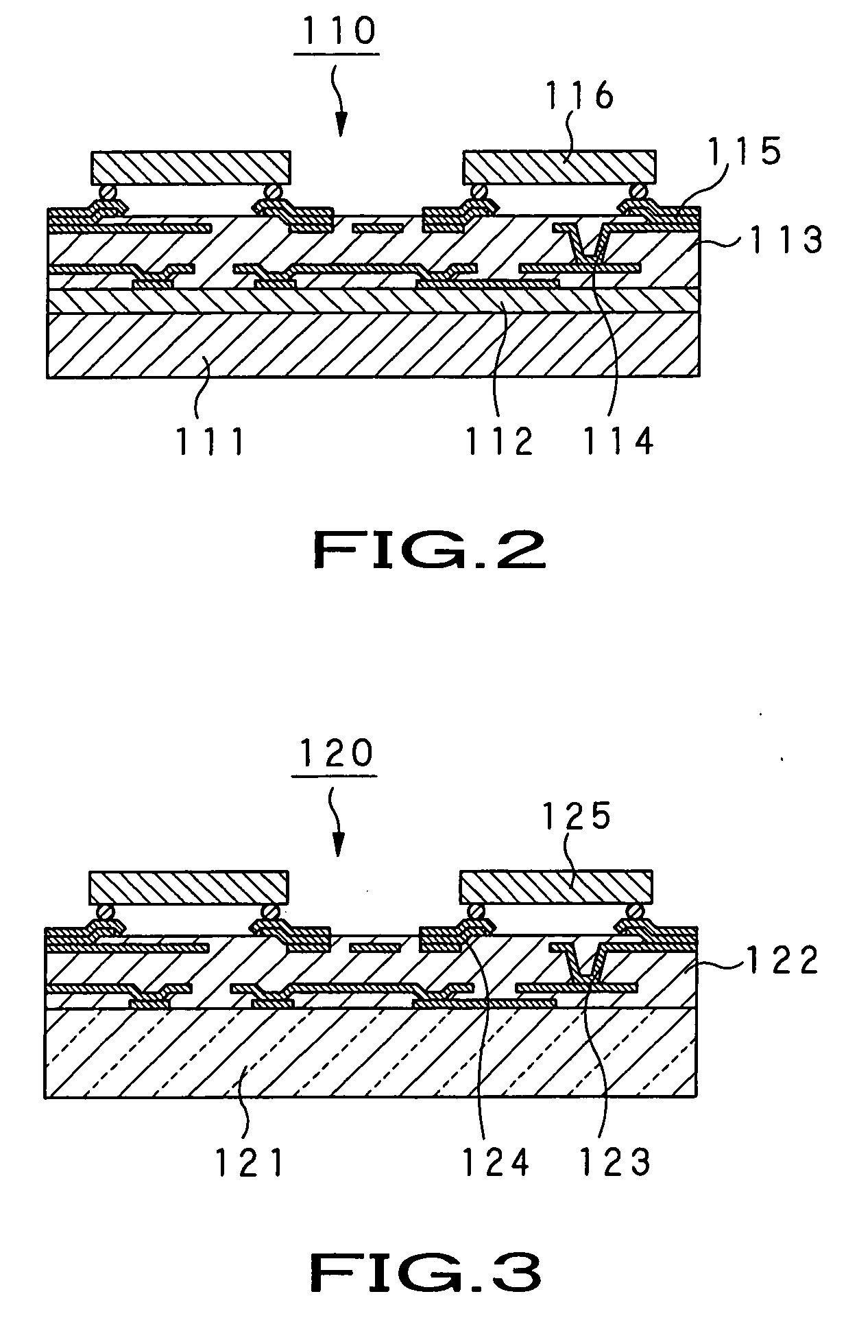
[0098] the high-frequency module according to the present invention will be described below with reference to FIG. 18. This high-frequency module is generally indicated with a reference 40. As shown in FIG. 18, the high-frequency module 40 has the base substrate block 2 in which a second organic substrate 41 using a woven glass fabric 42 as a core material is used in place of the aforementioned second organic substrate 12 as the lower layer.

[0099] Note that since the high-frequency module 40 shown in FIG. 18 is constructed of the same or similar components as or to those in the aforementioned high-frequency module 1 except for the second organic substrate 41, the components will be indicated with the same or similar references as or to those for the components in the high-frequency module 1 and will not be described in detail any more.

[0100] In the high-frequency module 40 in FIG. 18, the second organic substrate 41 formed from a both-side copper clad substrate is an integration of...

first embodiment

[0102] The high-frequency module 40 shown in FIG. 18 has electrical properties equal to those of the aforementioned high-frequency module 1 according to the present invention and also is designed to have an improved mechanical strength. The first organic substrate 11 and elements block 3 in the high-frequency module 40 in FIG. 18 can be formed from an organic material such as an acrylate resin, epoxy resin or polyolefin resin which will still remain relatively soft even after having been cured, for example. That is, the material for the first organic substrate 11 and elements block 3 can be selected with a higher freedom.

third embodiment

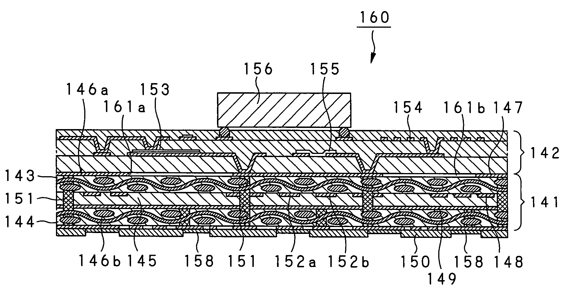
[0103] the high-frequency module according to the present invention will be described below with reference to FIG. 19. This high-frequency module is generally indicated with a reference 50 in FIG. 19. The high-frequency module 50 is formed by integrating first and second organic substrates 51 and 52 with a prepreg 53 laid between them, and stacking a third organic substrate 54 integrally on the first organic substrate 51 by build-up or one-operation pressing. The high-frequency module 50 uses a both-side copper clad substrate as the first organic substrate 51, having copper foil layers bonded to top and bottom main sides, respectively, thereof and which form first and second wiring layers 55 and 56, respectively, and also a both-side copper clad substrate as the second organic substrate 52, having copper foil layers bonded to top and bottom main sides, respectively, thereof and which form third and fourth wiring layers 57 and 58, respectively. Also, the high-frequency module 50 uses...


PUM

PropertyMeasurementUnit
Electrical conductoraaaaaaaaaa
Frequencyaaaaaaaaaa
Inductive effectaaaaaaaaaa

Abstract

A high-frequency module having a communication function is provided which includes a base substrate block (2) formed from organic substrates (11, 12), the organic substrate (11) having wiring layers (14, 15) formed on main sides, respectively, thereof while the organic substrate (12) has wiring layers (16, 17) formed on main sides, respectively, thereof, the base substrate block (2) having a buildup surface formed by flattening an uppermost layer, and an elements block (3) formed from organic insulative layers (26, 28) formed on the buildup surface of the base substrate block (2) and in which a plurality of conductive parts (19, 20, 32) forming passive elements and distributed parameter elements, which transmit a high-frequency signal, are formed along with wiring layers (27, 29). The conductive parts (19, 20, 32) in the elements block (3) are formed correspondingly to portions of the organic substrate (11) in the base substrate block (2) where no woven glass fabric is laid.

Description

TECHNICAL FIELD [0001] The present invention relates to a high-frequency module having functions of information communication and storage and which is to be installed fixedly or removably as an ultra-small communication module in an electronic device such as a personal computer, personal digital assistant, mobile phone or an audio device to provide an ultra-compact communication module, and a method of producing the high-frequency module. [0002] This application claims the priority of the Japanese Patent Application No. 2002-017620 filed on Jan. 25, 2002, the entirety of which is incorporated by reference herein. BACKGROUND ART [0003] Conventionally, audio or video information is digitized for easy treatment in a personal computer, various mobile electronic devices or the like. Namely, digital data can easily be recorded, reproduced or transmitted without being deteriorated in quality. Such digital audio or video information can have its frequency band compressed with the audio and ...

Claims


Application Information

Patent Timeline
IPC IPC(8): H01L23/12H01L23/14H01L23/498H01L23/66H01P1/00H05K1/02H05K1/03H05K1/16H05K3/46
CPCH01L23/145H01L2224/16225H01L23/66H01L2224/16237H01L2224/45015H01L2224/48091H01L2924/01004H01L2924/01078H01L2924/01079H01L2924/09701H01L2924/19105H01L2924/19107H01L2924/20752H01L2924/30107H01L2924/3025H05K1/024H05K1/0366H05K1/16H05K1/162H05K1/167H05K3/4602H05K3/4688H05K2201/029H05K2201/0352H05K2203/1581H01L23/49833H01L2924/01028H01L2924/01014H01L2924/01013H01L24/45H01L24/48H01L2924/00014H01L2924/12042H01L2924/14H01L2924/181H01L2924/00H01L2924/00012H01L2924/207H01L2224/45099H01L23/12H05K1/18H01P1/00
Inventor OKUBORA, AKIHIKO
Owner SONY CORP
Why Eureka
Try Eureka