HIGH TOLERANCE TCR BALANCED HIGH CURRENT RESISTOR FOR RF CMOS AND RF SiGe BiCMOS APPLICATIONS AND CADENCED BASED HIERARCHICAL PARAMETERIZED CELL DESIGN KIT WITH TUNABLE TCR AND ESD RESISTOR BALLASTING FEATURE

Inactive Publication Date: 2005-07-21
GLOBALFOUNDRIES INC
View PDF12 Cites 11 Cited by
  • Summary
  • Abstract
  • Description
  • Claims
  • Application Information

AI Technical Summary

Benefits of technology

[0019] It is an object of the present invention to provide a resistor structure that maintains structural and material integrity at high current and temperature, and has a low net thermal coefficient of resistance and a high melting temperature.
[0020] It is a further objective to provide a resistor structure that provides a uniform current within the structure and provides self-ballasting within the physical resistor structure to maintain a uniform current density within the resistor itself, especially at high frequencies including RF frequencies.
[0021] It is a further objective to provide a semiconductor resistor structure and method of fabrication that is customized to achieve a desired (optimized) TCR, and preferably, a low net Temperature Coefficient of Resistance (TCR) value at high currents and in a joule-heating regime of operation. To this end, it is advantageous to provide a semiconductor resistor element structure and method of fabrication for use in power amplifiers, and ESD circuit applications that provides a tunable Temperature Coefficient of Resistance for circuit linearity.

Problems solved by technology

Conventional metal resistor structures subjected to high currents above a critical current-to-failure point, can result in metal blistering, extrusion, and melting of the metal resistor regions.
Additionally, subjecting a conventional resistor to high current may result in a thermal gradient in the surrounding insulator that may exceed the yield stress and result in insulator cracking.
The above phenomena both reduce the integrity of the dielectric and semiconductor chips when subjected to high current.
Source and drain resistance are lowered using salicide regions on the source and drain diffusion regions, but salicide near the gate impacts the ESD robustness of the device.
It is also well known that current drive in devices at high current is not uniform, largely due to non-uniform temperature distribution in such devices when driven at high currents.
This design practice does not allow for the flexibility needed for RF applications.
A difficulty in the design of RF ESD solutions is that traditionally, specific designs are fixed in size in order to achieve verifiable ESD results for a technology.
The difficulty with analog and RF technology is that a wide range of circuit applications exists where one ESP size structure is not suitable due to loading of the circuit.
A second issue is that the co-synthesis of the circuit and the circuit must be done to properly evaluate the RF performance objectives of a resistor element.
A third issue for RF mixed signal designs, there are analog and digital circuits.

Method used


Image

  • HIGH TOLERANCE TCR BALANCED HIGH CURRENT RESISTOR FOR RF CMOS AND RF SiGe BiCMOS APPLICATIONS AND CADENCED BASED HIERARCHICAL PARAMETERIZED CELL DESIGN KIT WITH TUNABLE TCR AND ESD RESISTOR BALLASTING FEATURE
  • HIGH TOLERANCE TCR BALANCED HIGH CURRENT RESISTOR FOR RF CMOS AND RF SiGe BiCMOS APPLICATIONS AND CADENCED BASED HIERARCHICAL PARAMETERIZED CELL DESIGN KIT WITH TUNABLE TCR AND ESD RESISTOR BALLASTING FEATURE
  • HIGH TOLERANCE TCR BALANCED HIGH CURRENT RESISTOR FOR RF CMOS AND RF SiGe BiCMOS APPLICATIONS AND CADENCED BASED HIERARCHICAL PARAMETERIZED CELL DESIGN KIT WITH TUNABLE TCR AND ESD RESISTOR BALLASTING FEATURE

Examples


Embodiment Construction

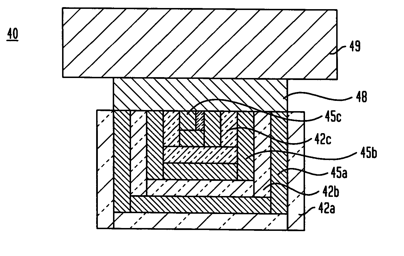
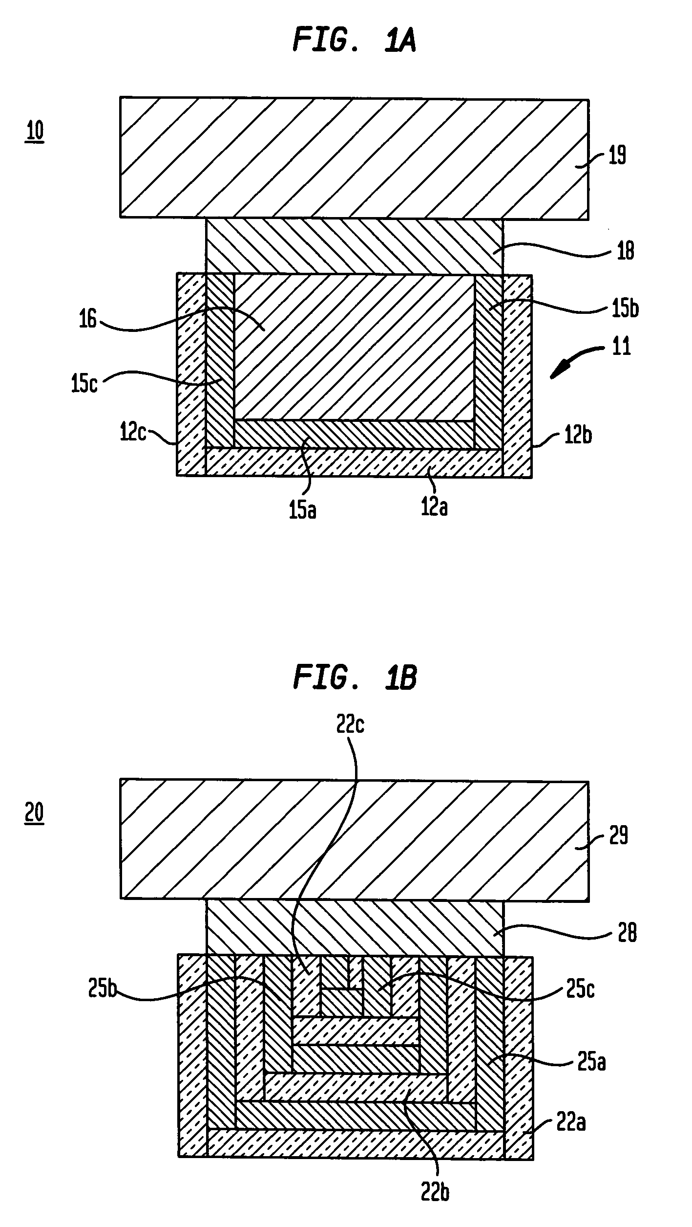
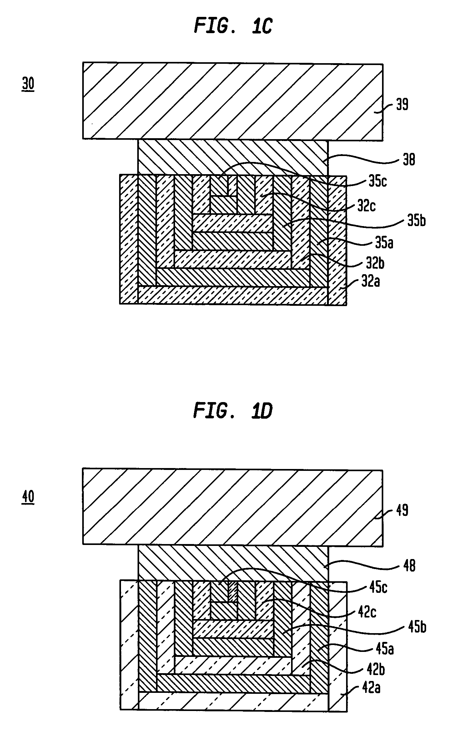
[0042] Referring now to the drawings, and more particularly to FIG. 1(a), there is depicted a novel resistive structure 10 according to a first embodiment of the invention. In this embodiment, the resistive structure 10 is formed in a trough 11, for example, formed in a substrate (not shown) having a layer of dielectric material conforming to the base and sidewalls. The trough structure 11 comprises a bottom portion of dielectric material 12a and two parallel sidewall formations 12b, 12c of dielectric material. Examples of insulative dielectric materials for the portions 12a-12c include, but are not limited to: low-k materials, SiLK®, an oxide, nitride, oxynitride or any combination thereof including multilayers, porous or non-porous inorganic and / or organic dielectrics formed by a deposition process such as CVD, PECVD, chemical solution deposition, atomic layer deposition and other like deposition processes. Thus, the dielectric material may be comprised of SiN, SiO2, a polyimide p...


PUM


Abstract

A resistor device structure and method of manufacture therefore, wherein the resistor device structure invention includes a plurality of alternating conductive film and insulative film layers, at least two of the conductive film layers being electrically connected in parallel to provide for high current flow through the resistor device at high frequencies with increased temperature and mechanical stability. The alternating conductive film and insulative film layers may be of a planar or non-planar geometric spatial orientation. The alternating conductive film and insulative film layers may include lateral and vertical portions designed to enable a uniform current density flow within the structure itself through a self-ballasting effect within the physical resistor. A computer aided design tool with graphical and schematic features is provided to enable generation of hierarchical parameterized cells for a resistor element with the ability to provide customization, personalization and tunability of TCR, TCR matching, and high current and ESD robustness.

Description

BACKGROUND OF INVENTION [0001] 1. Field of the Invention [0002] The present invention relates to semiconductor devices and methods of manufacturing thereof, and more particularly to a semiconductor resistor structure optimized for tolerance and high current and a method of fabrication thereof. More specifically, the present invention provides a high tolerance Temperature Coefficient of Resistance (TCR) balanced high current resistor for RF CMOS and RF SiGe BiCMOS applications and a computer aided design kit for designing the same. [0003] 2. Background of the Invention [0004] Optimization of passive elements for tolerance and high current is valuable for RF technologies. In RF circuit applications, precision resistors are needed for I / O circuitry implementing both radio frequency (RF) CMOS an RF SiGe technology. High tolerance resistors are important for accurate prediction of models and statistical control. Moreover, in RF devices and circuits, high tolerance resistors are needed th...

Claims


Application Information

Patent Timeline
IPC IPC(8): H01C7/06H01L21/02H01L21/20H01L23/62H01L27/02H01L27/08H01L29/00
CPCH01C7/06H01L27/0288H01L27/0802H01L28/24H01L2924/0002H01L2924/00
Inventor ESHUN, EBENEZER E.VOLDMAN, STEVEN H.
Owner GLOBALFOUNDRIES INC
Why Eureka
Try Eureka