Periodic patterns and technique to control misalignment between two layers
a technology of two layers and periodic patterns, applied in the field of metalrology systems, can solve the problems of limited optical microscope accuracy, reworked or discarded semiconductor wafers, and malfunction of electronic devices fabricated, and achieve the effects of high sensitivity, high linearity, and high sensitivity
- Summary
- Abstract
- Description
- Claims
- Application Information
AI Technical Summary
Benefits of technology
Problems solved by technology
Method used
Image
Examples
Embodiment Construction
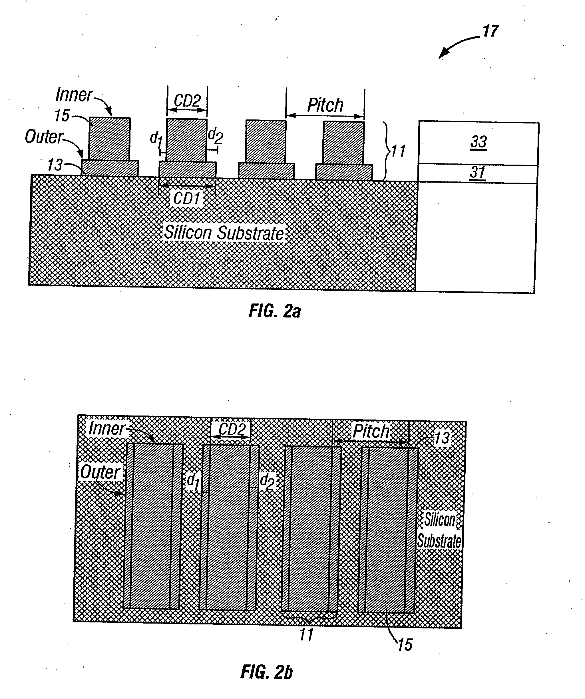
[0027]FIG. 2a is a cross-sectional view of a target 11 comprising two periodic structures 13, 15 on two layers 31, 33 of a device 17. The second periodic structure 15 is overlying or interlaced with the first periodic structure 13. The layers and the periodic structures may be at the same or different heights. The device 17 can be any device of which the alignment between two layers, particularly layers having small features on structures, needs to be determined. These devices are typically semiconductor devices; thin films for magnetic heads for data storage devices such as tape recorders; and flat panel displays.
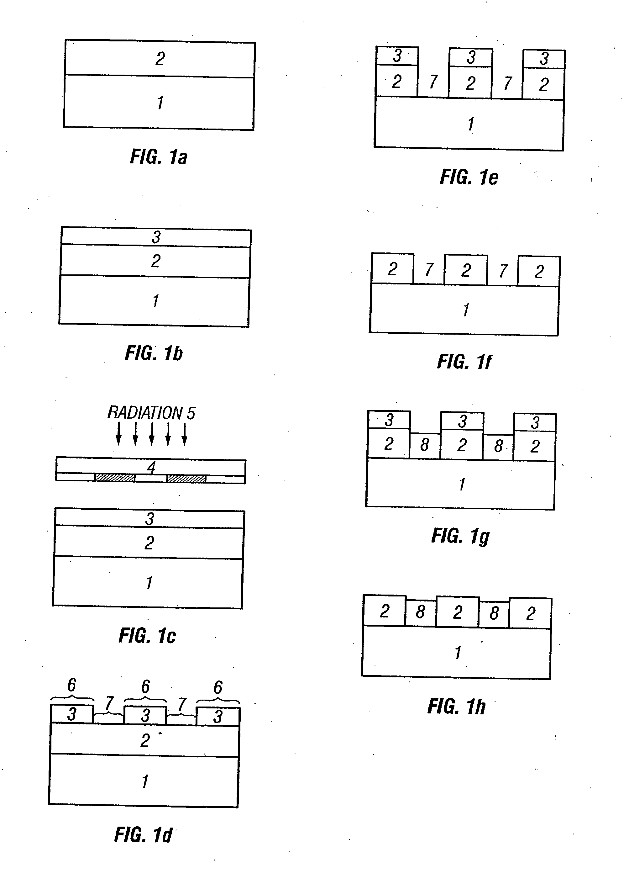
[0028] As shown in FIGS. 1a-1h, a device 17 is generally formed in a basic series of steps for each layer. First, as shown in FIG. 1a, a layer 2 is formed on a semiconductor substrate 1. The layer 2 may be formed by oxidization, diffusion, implantation, evaporation, or deposition. Second, as shown in FIG. 1b, resist 3 is deposited on the layer 2. Third, as shown in FIG. 1...
PUM
 Abstract
Description
Claims
Application Information
 - R&D
- Intellectual Property
- Life Sciences
- Materials
- Tech Scout
- Unparalleled Data Quality
- Higher Quality Content
- 60% Fewer Hallucinations
Browse by: Latest US Patents, China's latest patents, Technical Efficacy Thesaurus, Application Domain, Technology Topic, Popular Technical Reports.
© 2025 PatSnap. All rights reserved.Legal|Privacy policy|Modern Slavery Act Transparency Statement|Sitemap|About US| Contact US: help@patsnap.com


