Semiconductor device containing dielectrically isolated PN junction for enhanced breakdown characteristics
a dielectric isolation and semiconductor technology, applied in semiconductor devices, diodes, electrical devices, etc., can solve the problems reducing the on-resistance of the mosfet, and achieve the effect of increasing the avalanche breakdown voltage of the device, reducing the on-resistance of the mosfet, and increasing the cell packing density
- Summary
- Abstract
- Description
- Claims
- Application Information
AI Technical Summary
Benefits of technology
Problems solved by technology
Method used
Image
Examples
Embodiment Construction
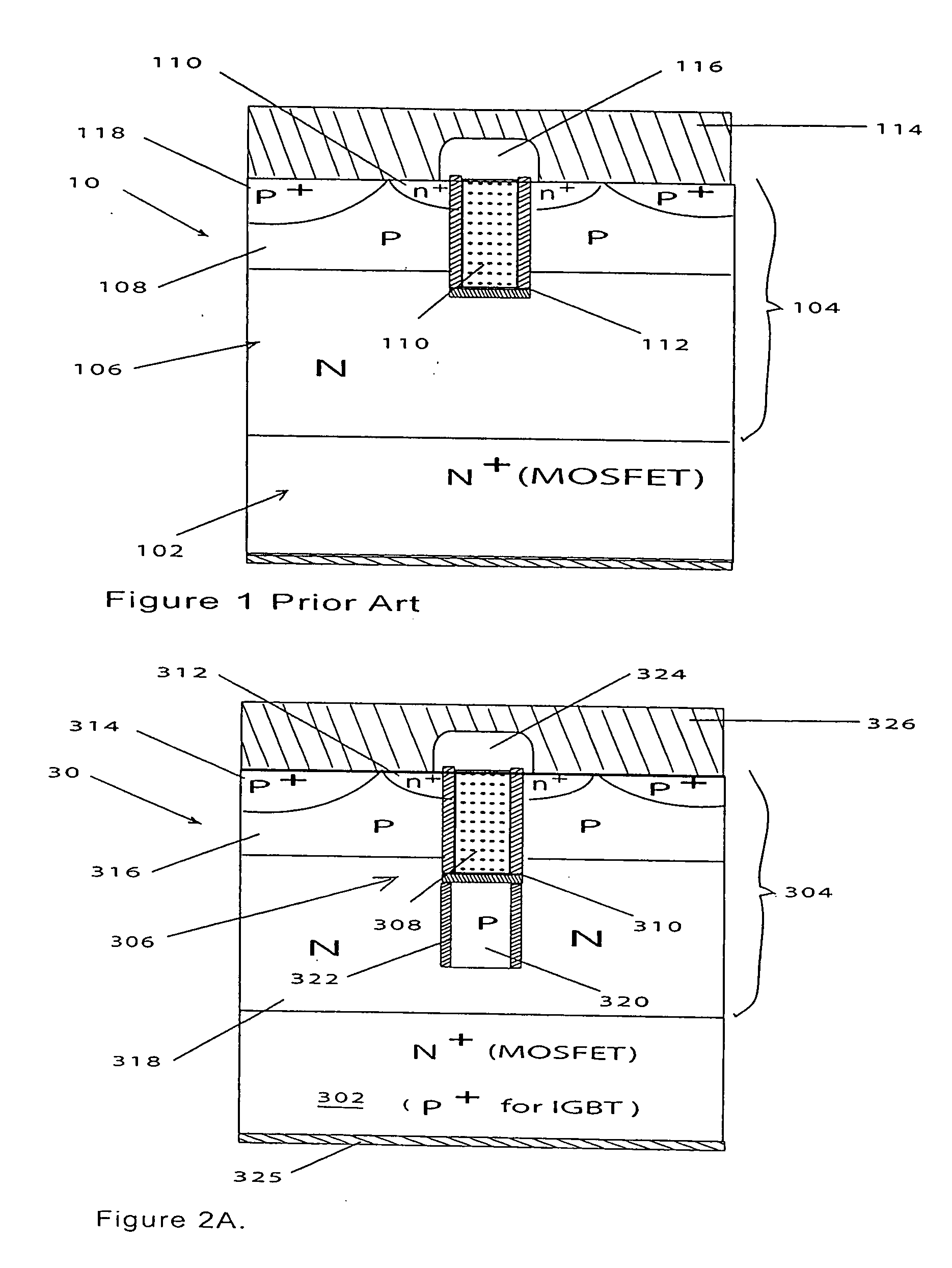
[0033]FIG. 2A shows a MOSFET 30 in accordance with this invention. MOSFET 30 is formed on an N+ substrate 302 and an overlying epi layer 304. Trenches 306 are formed in epi layer 304, and trenches 306 are lined with a gate oxide (SiO2) layer 310 and filled with a gate 308. Alternatively, layer 310 could be formed of silicon nitride (Si3N4). Gate 308 is typically formed of heavily-doped polysilicon and can include a silicide.
[0034] A mesa between trenches 306 includes a P− body region 316. Within P− body region 316 are N+ source regions 312 and a P+ body contact region 314. The top surface of gate 308 is covered with a BPSG layer 324. A source metal layer 326S overlies BPSG layer 324 and makes electrical contact with N+ source regions 312 and P+ body contact regions 314. Similarly, a metal layer 325 contacts N+ substrate 302, which functions as the drain. The electrical contact between metal layer 325 and N+ substrate 302 could be ohmic or could include a Schottky barrier.
[0035] Th...
PUM
 Abstract
Description
Claims
Application Information


