Method of controlling semiconductor device, signal processing method, semicondcutor device, and electronic apparatus

a semiconductor device and semiconductor technology, applied in the direction of radiation controlled devices, still video cameras, television systems, etc., can solve the problems of increasing the number of pixels and increasing the speed of imaging, affecting the dynamic range of the image, and affecting the image quality. , to achieve the effect of preventing the setting of a gain exceeding the dynamic range, extending the dynamic range, and favorable s/n ratio

Inactive Publication Date: 2005-08-04
SONY CORP
View PDF8 Cites 93 Cited by
  • Summary
  • Abstract
  • Description
  • Claims
  • Application Information

AI Technical Summary

Benefits of technology

[0030] The present invention has been made in view of the situation described above, and an object thereof is to provide techniques relating to column-based circuits that allow a dynamic range to be extended while maintaining favorable S / N ratio, preferably preventing setting of a gain exceeding the dynamic range.

Problems solved by technology

Since these amps are analog amps, thermal noise, which is analog random noise, could occur.
An increased bandwidth is needed in the proximity of the output amp 950, and thermal noise that could be generated by amps tends to increase as the bandwidth increases.
This is disadvantageous considering the trend of increased number of pixels and increased speed of imaging.
When the bit precision of the A / D converter 970 is increased, power consumption is increased, and noise caused by the circuitry itself prohibits improvement in bit precision.
Thus, in a column-based image sensor according to the related art, it has been difficult to improve bit precision, and to extend dynamic range while maintaining favorable S / N ratio.
In that case, however, the construction of each of the pixels becomes complex, so that the advantages of reduced cost and reduced size due to the column-based arrangement are lost.
Furthermore, according to the techniques disclosed in the documents, depending on the constructions of the PGA circuits or circuits provided at subsequent stages thereof, in some cases, signal levels amplified by adjusted gains exceed the dynamic range of the circuitry, failing to appropriately extend the dynamic range of signals.

Method used


Image

  • Method of controlling semiconductor device, signal processing method, semicondcutor device, and electronic apparatus
  • Method of controlling semiconductor device, signal processing method, semicondcutor device, and electronic apparatus
  • Method of controlling semiconductor device, signal processing method, semicondcutor device, and electronic apparatus

Examples


first and second embodiments

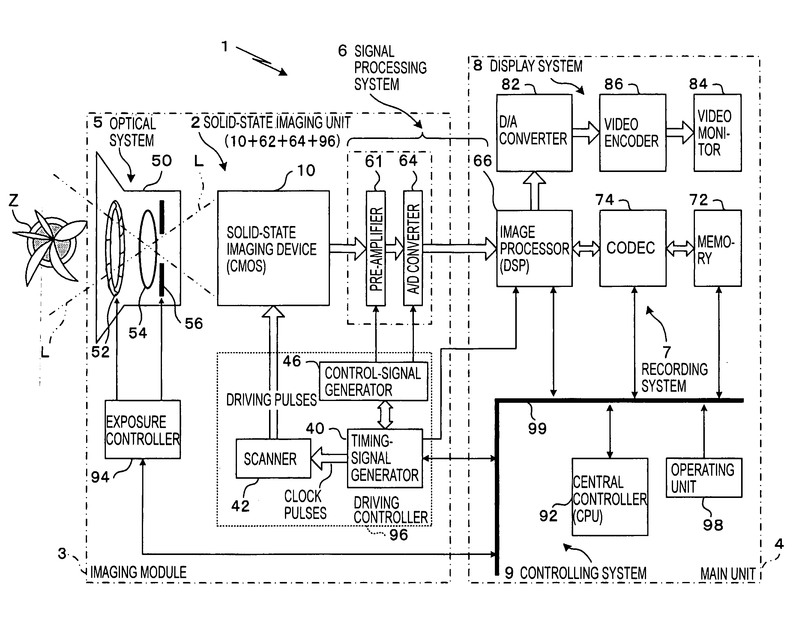
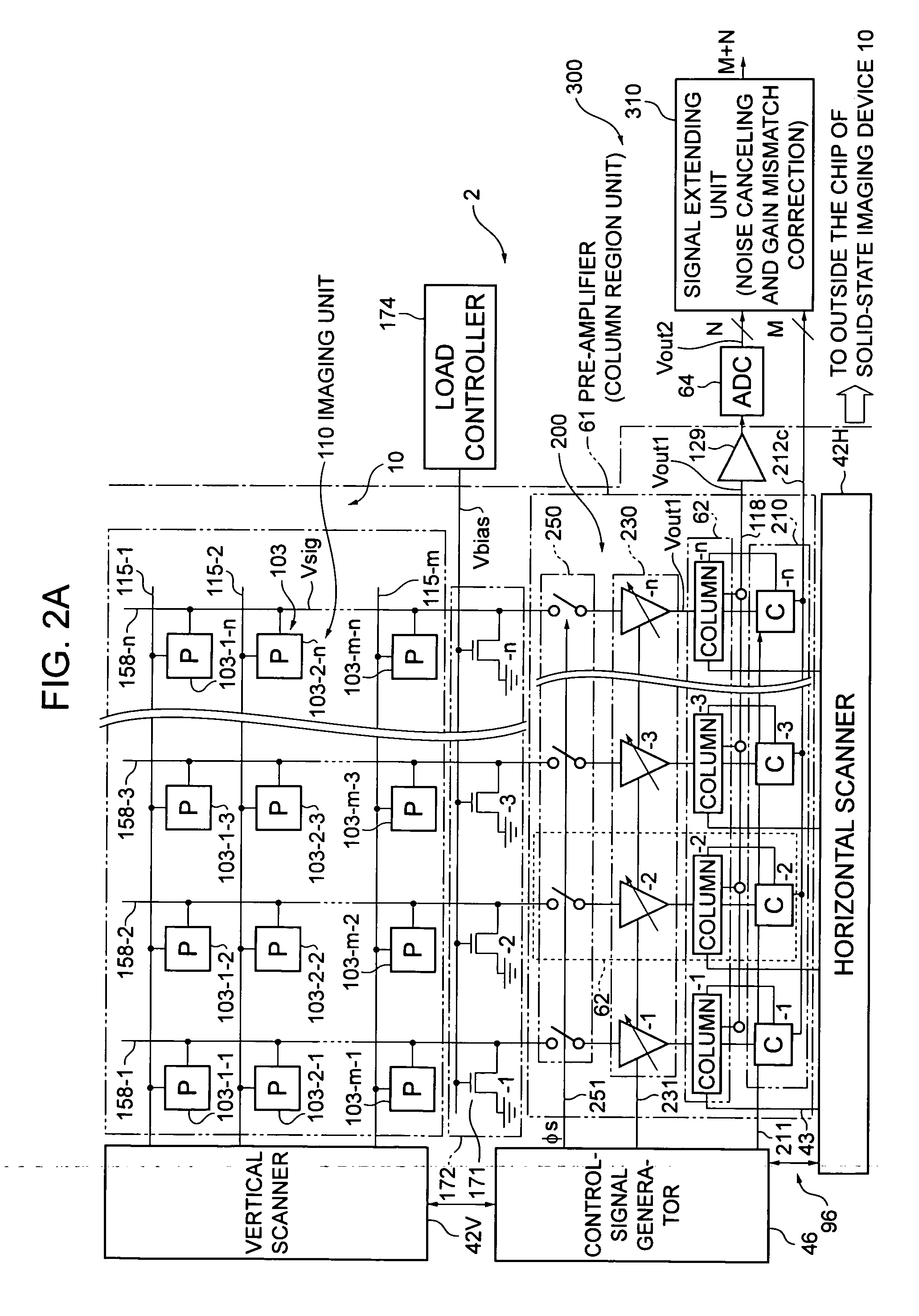
[0088]FIGS. 2A and 3 are schematic diagrams showing the solid-state imaging unit 2 mainly composed of the CMOS solid-state imaging device 10, and peripheral parts thereof, according to first and second embodiments of the present invention. In the embodiments shown in FIGS. 2A and 3, the solid-state imaging device 10 is composed mainly of the imaging unit 110 and the pre-amplifier 61, and the A / D converter 64 is provided externally to the solid-state imaging device 10.

[0089] The solid-state imaging device 10 is implemented by forming the imaging unit 110 and the pre-amplifier 61 on a common semiconductor substrate. Furthermore, the A / D converter 64 and a signal extending unit 310 may be formed on the same chip, in regions where column regions of the solid-state imaging device 10 are not formed. In that case, the solid-state imaging unit 2 is substantially coincides with the solid-state imaging device 10.

[0090] The solid-state imaging unit 2 includes an imaging unit (a photoelectric...

second embodiment

First Example of Operation Timing and Detecting Circuit, Which Relates to the Second Embodiment

[0140]FIG. 4 is a timing chart showing operation timing in one horizontal period of the solid-state imaging unit 2 according to the second embodiment shown in FIG. 3. FIG. 5 is diagram showing an example construction of a pixel-signal detector 210 in the second embodiment shown in FIG. 3.

[0141] As shown in FIG. 5, the pixel-signal detector 210 in the second embodiment includes a pixel-signal-level detector 213 and a classification-signal generator 224. The pixel-signal-level detector 213 detects the level of a pixel signal Vsig output through a vertical signal line 158 of the imaging unit 110, and compares the level with predetermined threshold values. The classification-signal generator 224 generates a classification signal Vsepa for classifying the level of the pixel signal Vsig based on a result of detection by the pixel-signal-level detector 213.

[0142] The pixel-signal-level detector...

first embodiment

Second Example of Operation Timing and Detecting Circuit, Which Relates to the First Embodiment

[0168]FIG. 7 is a timing chart showing operation timing during a horizontal period of the solid-state imaging unit2 according to the first embodiment shown in FIG. 2A. FIG. 8 is a diagram showing an example construction of the pixel-signal detector 210 in the first embodiment shown in FIG. 2A.

[0169] Next, the operation of the pixel-signal detector 210 in the first embodiment will be described using specific examples of numeric values. For example, in an arrangement according to the first embodiment in which the signal voltage Vout is compared with predetermined reference voltages on the output side of the pixel-signal amplifier 230, when gain setting is controlled by three levels of ×2, ×4, and ×8 based on powers of 2, the reference voltages are 500 mV, 250 mV, and 125 mV. In order to perform comparisons with these reference voltages, the pixel-signal detector 210 receives comparison volt...


PUM


Abstract

A pre-amplifier (column region unit) of a solid-state imaging device includes a pixel-signal controller. The pixel-signal controller, for each vertical signal line, detects the level of each pixel signal independently by a pixel-signal detector on the output side of a pixel-signal amplifier, and sets a gain independently to the pixel-signal amplifier according to the level of the signal. At a subsequent stage of the solid-state imaging device, an analog-to-digital (A/D) converter and a signal extending unit are provided. The A/D converter digitizes a pixel signal, and the digitized pixel signal is corrected by a gain set to the pixel-signal amplifier with reference to a classification signal from the pixel-signal detector, so that the dynamic range of signals of one screen is extended.

Description

BACKGROUND OF THE INVENTION [0001] 1. Field of the Invention [0002] The present invention relates to a semiconductor device including a plurality of unit elements, an electronic apparatus including the semiconductor device, and a controlling method and a signal processing method relating to the semiconductor device or the electronic apparatus. [0003] More specifically, the present invention relates to a semiconductor device (e.g., a solid-state imaging device) for detecting distribution of a physical quantity by reading electric signals representing the distribution of the physical quantity obtained by a matrix of unit elements (e.g., unit pixels) that are sensitive to electromagnetic waves input from the outside, such as light or radiation, a method of controlling gains for signals in the semiconductor device, and signal processing techniques for output signals amplified by the controlled gains. [0004] 2. Description of the Related Art [0005] Semiconductor devices for detecting dis...

Claims


Application Information

Patent Timeline
Patent Type & Authority Applications(United States)
IPC IPC(8): H04N5/243H01L27/146H04N5/335H04N5/355H04N5/369H04N5/374H04N5/376H04N5/378H04N101/00
CPCH04N5/243H04N5/3575H04N5/3696H04N5/37457H04N5/37455H04N23/76H04N25/616H04N25/702H04N25/772H04N25/778H04N25/76H04N25/75
Inventor SUMI, HIROFUMINAKAMURA, NOBUOKAWAHITO, SHOJI
Owner SONY CORP
Why Eureka
Try Eureka