Apparatus for characterization of photoresist resolution, and method of use

a technology of photoresist film and apparatus, which is applied in the field of apparatus for characterization of photoresist film resolution, can solve the problems of limiting the usefulness of the method, the inability to easily integrate the means used to generate a sinusoidal optical grating in a photoresist film with standard photolithographic tools, and the increasing stringent requirements of the lithographic imaging system. , to achieve the effect of efficient characterizing the spatial response and facilitating the automatic evaluation

Inactive Publication Date: 2005-08-04
GLOBALFOUNDRIES INC
View PDF13 Cites 27 Cited by
  • Summary
  • Abstract
  • Description
  • Claims
  • Application Information

AI Technical Summary

Benefits of technology

[0011] An apparatus and method are described for efficiently characterizing the spatial response of a photoresist film. Conventional projection lithographic tools may be advantageously adapted to simultaneously generate both interferometrically and conventionally imaged optical patterns in a resist on a wafer. Thus, it is possible to simultaneously project onto the wafer (i.e., in the same exposure step) many sets of sinusoidal grating patterns of various spatial frequencies as well as non-periodic, arbitrarily shaped features that may serve as alignment marks (also termed “fiducial” marks). These marks facilitate the automated evaluation of the developed photoresist patterns (e.g., using CD-SEM or Critical Dimension-Scanning Electron Microscope). The measured linewidths can then be analyzed to extract the modulation transfer function (MTF), and thus the line-spread function (LSF), for the photoresist under a specific set of processing conditions.
[0012] Preferred embodiments and methods disclosed herein make use of an optical arrangement that integrates interferometric and conventional methods for patterning the photoresist. The photoresist advantageously resides on a wafer positioned in a standard lithographic tooling apparatus, so that photoresist on a wafer may be exposed to a full set of grating patterns having different spatial frequencies, thereby eliminating errors due to drift in process conditions which would otherwise arise if each grating pattern were printed on a separate wafer.

Problems solved by technology

As photolithographic techniques have succeeded in producing ever smaller feature sizes, the demands on the performance of the lithographic imaging system have become increasingly stringent.
In particular, the intrinsic ability of the photoresist film, which may be regarded as an element in the imaging system, to resolve small features has become a matter of great concern, since the inherent resolution of a photoresist places a limit on the dimension of the smallest feature that can be produced.
Unfortunately, the means used to generate a sinusoidal optical grating in a photoresist film can not be easily integrated with standard photolithographic tools, and this incompatibility greatly limits the usefulness of the method of Hoffnagle et al. described above.
This approach is impractical for high spatial frequencies and short wavelengths, because of the difficulty of accurately patterning the reticle substrate with a semitransparent material having precisely controlled optical density.
Consequently, there is at present no suitable method for generating sinusoidal optical gratings using conventional lithographic tools.

Method used


Image

  • Apparatus for characterization of photoresist resolution, and method of use
  • Apparatus for characterization of photoresist resolution, and method of use
  • Apparatus for characterization of photoresist resolution, and method of use

Examples


Embodiment Construction

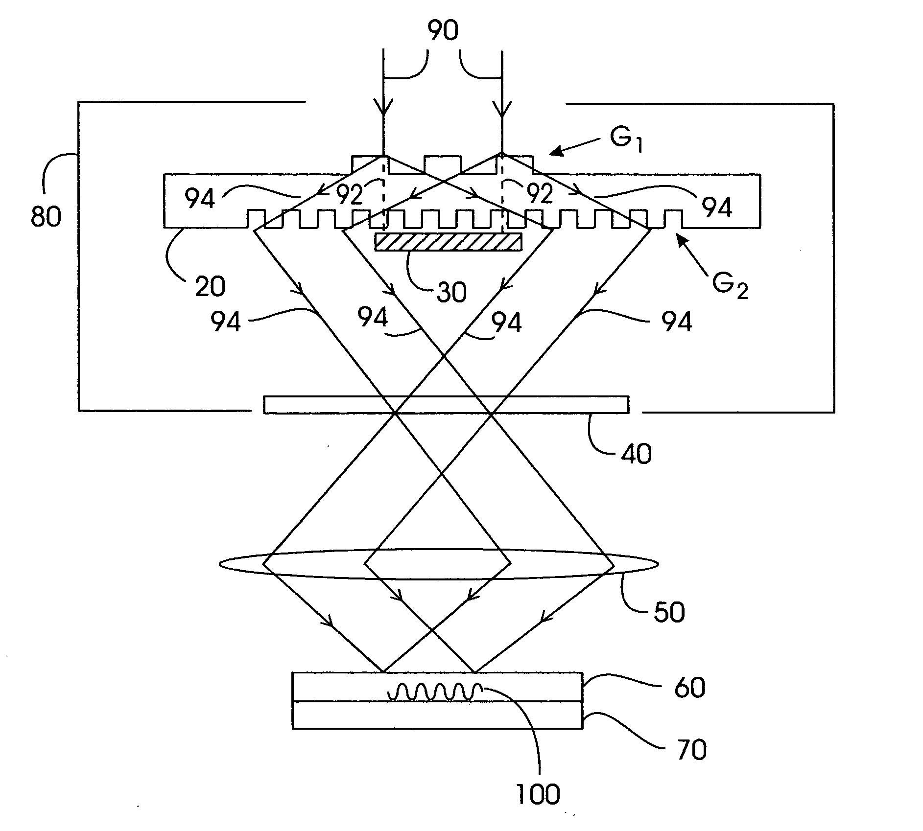
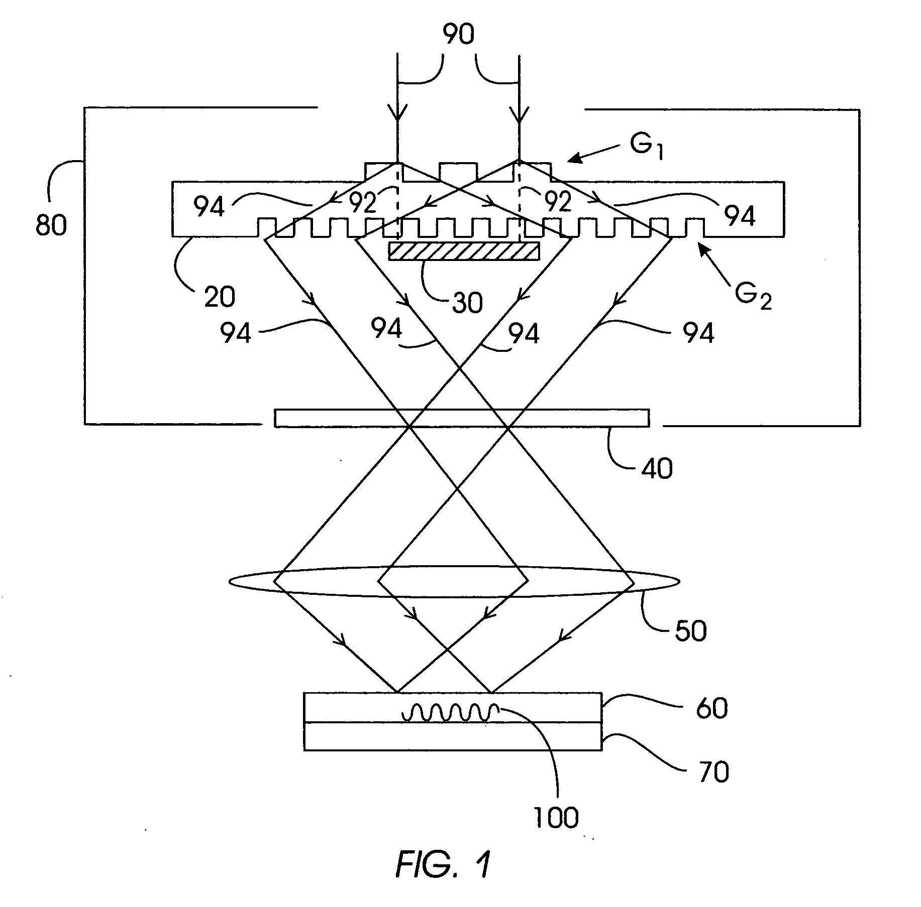
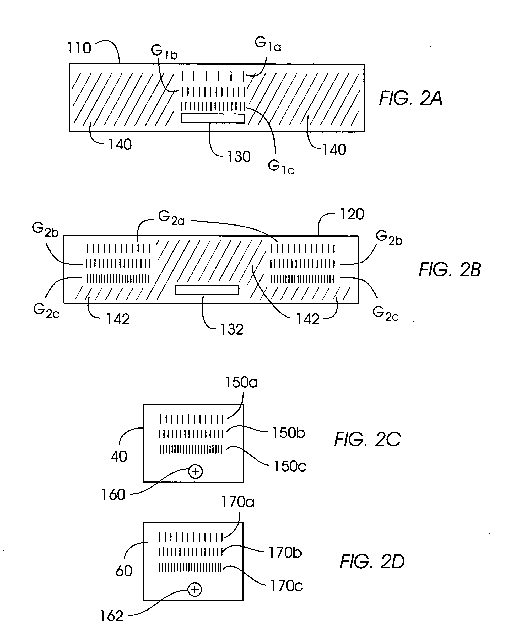
[0022] A diffraction grating may be used to split a beam of light into mutually coherent beams, corresponding to the propagating diffraction orders of the grating. If the grating is placed in the reticle plane of a lithographic projection system, the beams corresponding to the various diffraction orders originating at any single point on the grating recombine at the wafer plane of the system. The angles of incidence of these beams with respect to the normal at the wafer are determined by the pitch of the diffraction grating and the magnification of the projection optics.

[0023] If a reticle could be fabricated in such a way as to function as a diffraction grating with only two diffracted orders, each of which had the same intensity and propagated symmetrically with respect to the normal to the reticle, then the projection optics would function essentially as an interferometer, thereby generating a sinusoidal optical grating pattern in the photoresist film at the wafer plane. However...


PUM

PropertyMeasurementUnit
wavelengthaaaaaaaaaa
thicknessaaaaaaaaaa

Abstract

An optical apparatus used for the efficient characterization of photoresist material includes at least one grating interferometer having at least two gratings that together define an optical recombination plane. An optical stop blocks any zeroth order beam from propagating through the apparatus. A reticle positioned at the recombination plane has at least one fiducial marking therein. A lithographic imaging optical tool is positioned so that its input optical plane is substantially coincident with the optical recombination plane and its output imaging plane is substantially coincident with photoresist on a wafer. The apparatus writes in the photoresist latent, sinusoidal grating patterns, preferably of different spatial frequencies, as well as at least one fiducial mark whose pattern is determined by the marking in the reticle. After the photoresist is developed, its intrinsic spatial resolution may be determined by automated means.

Description

TECHNICAL FIELD [0001] The invention relates to an apparatus and method for characterizing the resolution of a radiation sensitive medium such as a photoresist. More particularly, the invention is directed to an interferometric optical arrangement for accomplishing this characterization. BACKGROUND [0002] As photolithographic techniques have succeeded in producing ever smaller feature sizes, the demands on the performance of the lithographic imaging system have become increasingly stringent. In particular, the intrinsic ability of the photoresist film, which may be regarded as an element in the imaging system, to resolve small features has become a matter of great concern, since the inherent resolution of a photoresist places a limit on the dimension of the smallest feature that can be produced. Accordingly, the quantitative characterization of a photoresist's spatial response is important for resolution-enhancing technologies such as optical proximity correction (OPC), phase-shifti...

Claims


Application Information

Patent Timeline
Patent Type & Authority Applications(United States)
IPC IPC(8): G03F7/20
CPCG03F7/70108Y10S430/143G03F7/70608
Inventor HINSBERG, WILLIAM DINAN IIIHOFFNAGLE, JOHN ALLENHOULE, FRANCES ANNESANCHEZ, MARTHA INEZ
Owner GLOBALFOUNDRIES INC
Why Eureka
Try Eureka