Method for manufacturing thin film transistor array panel for display device

a technology of thin film transistor array panel and manufacturing method, which is applied in the direction of optics, instruments, electrical equipment, etc., can solve the problems of deterioration of adhesiveness between the organic insulating layer and the ito film, and achieve the effect of minimizing contact resistance and good adhesiveness

Inactive Publication Date: 2005-08-04
SAMSUNG DISPLAY CO LTD
View PDF10 Cites 12 Cited by
  • Summary
  • Abstract
  • Description
  • Claims
  • Application Information

AI Technical Summary

Benefits of technology

[0010] It is an object of the present invention to provide a TFT array panel and a manufacturing method thereof having good adhesiveness betw...

Problems solved by technology

However, adhesiveness between the organic insulating layer and the ITO film is deteriora...

Method used


Image

  • Method for manufacturing thin film transistor array panel for display device
  • Method for manufacturing thin film transistor array panel for display device
  • Method for manufacturing thin film transistor array panel for display device

Examples


first embodiment

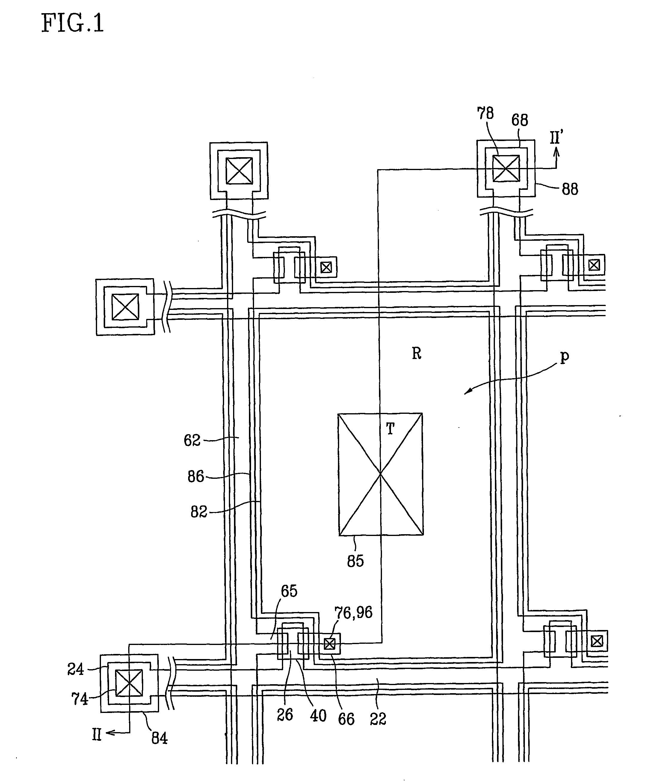
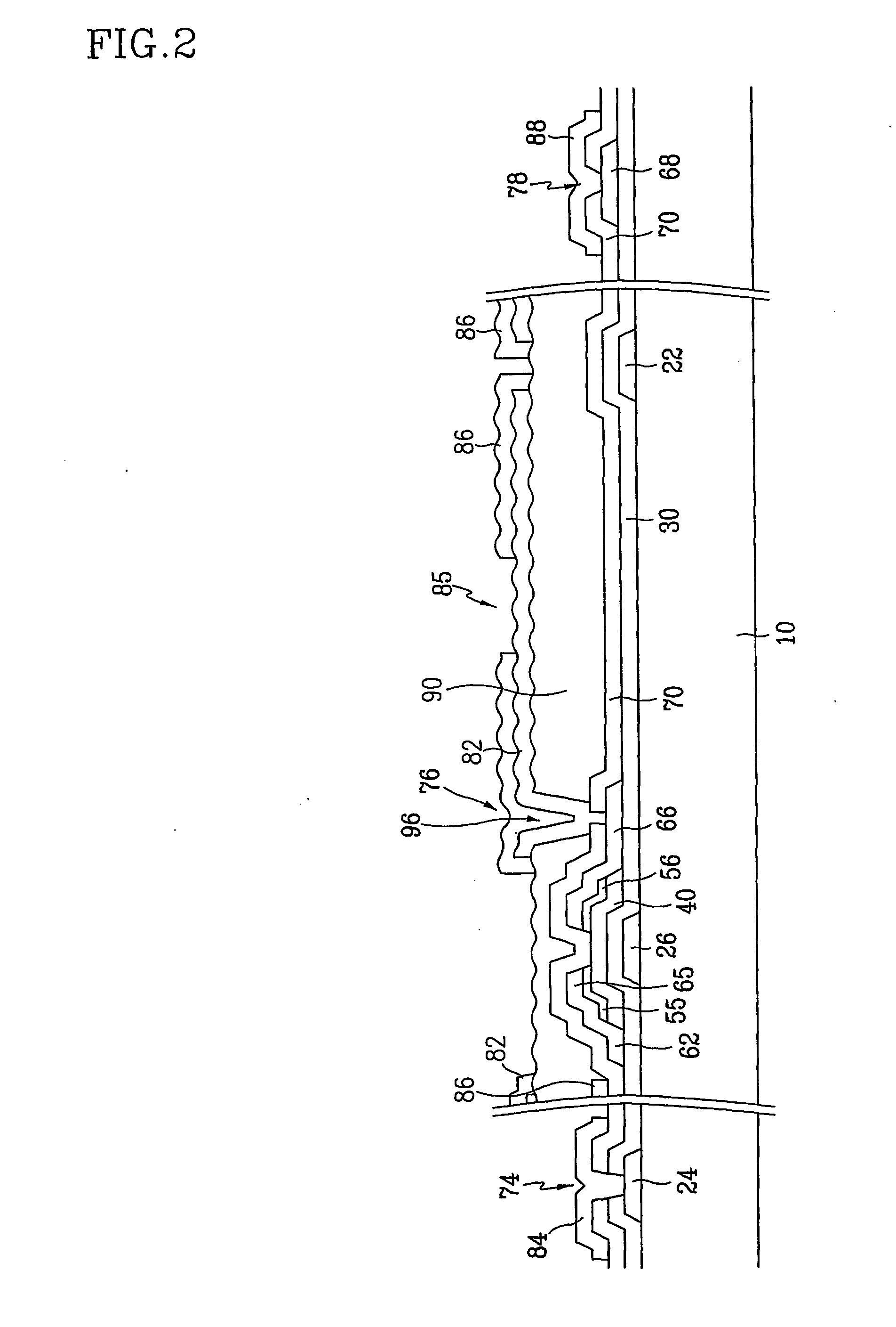
[0042] First, a transflective type LCD according to the present invention will be described in detail with reference to FIGS. 1 and 2.

[0043]FIG. 1 is a layout view of a TFT array panel for a transflective type LCD according to a first embodiment of the present invention, and FIG. 2 is a sectional view of the TFT array panel shown in FIG. 1 taken along the line II-II′.

[0044] A gate wire is formed on an insulating substrate 10. The gate wire includes either a single layer preferably made of Ag, Ag alloy, Al and Al alloy having low resistivity, or multiple layers including the single layer. The gate wire includes a plurality of gate lines 22 extending substantially in a transverse direction, a plurality of gate pads 24 connected to one ends of the gate lines 22 for receiving gate signals from external devices and transmitting the gate signals to the gate lines 22, and a plurality of gate electrodes 26 of TFTs connected to the gate lines 22. The gate wire may overlap pixel electrodes 8...

second embodiment

[0067] A TFT array panel for a reflective type LCD according to the present invention will be described in detail with reference to FIGS. 10 and 11.

[0068] As shown in FIGS. 10 and 11, the structure is almost the same as the structure according to the first embodiment.

[0069] However, different from the first embodiment, a plurality of reflecting films 86 are located directly on an organic insulating layer 90 and in direct electrical connection with a plurality of drain electrodes 66 through a plurality of contact holes 76 and 96. In addition, the reflecting film 86 occupies the entire pixel area.

[0070] Moreover, a plurality of gate wire 22, 24 and 26 and a plurality of data wire 62, 65 and 66 overlap relevant pixel electrodes 82 via the organic insulating layer 90 with low dielectric constant to give maximum aperture ratio.

[0071] Furthermore, a data wire 62, 65, 66 and 68 includes a conductor pattern 64 for storage capacitors overlapping the gate lines 22, and the pixel electrodes...

fourth embodiment

[0076]FIG. 12 is a layout view of a TFT array panel for an LCD according to the present invention, and FIGS. 13 and 14 are sectional views of the TFT array panel shown in FIG. 12 taken along the line XIII-XIII′ and the line XIV-XIV′ of FIG. 12, respectively.

[0077] As in the second embodiment, a gate wire is formed on an insulating substrate 10. The gate wire is preferably made of a material with low resistivity such as Ag, Ag alloy, Al and Al alloy. The gate wire includes a plurality of gate lines 22, a plurality of gate pads 24, and a plurality of gate electrodes 26. The gate wire further includes a plurality of storage electrodes 28 formed on the substrate, which are substantially parallel to the gate lines 22 and applied with a predetermined voltage such as a common voltage from an external source, which is also applied to a common electrode of an upper panel. The storage electrodes 28 overlap a storage capacitor conductor pattern connected to pixel electrodes 82, which will be d...


PUM


Abstract

A gate wire including gate lines, gate electrodes, and gate pads and extending in a transverse direction is formed on a substrate. A gate insulating layer is formed thereafter, and a semiconductor layer and an ohmic contact layer are sequentially formed thereon. A conductive material is deposited and patterned to form a data wire inducing data lines intersecting the gate lines, source electrodes, drain electrodes, and data pads. A protective layer made of silicon nitride is deposited on the substrate, and an organic insulating layer made of a photosensitive organic insulating material is coated on the protective layer. The organic insulating layer is patterned to form an unevenness pattern on its surface and first contact holes exposing the protective layer opposite the drain electrodes. Subsequently, the surface of the organic insulating layer is treated using inactive gas such as Ar, and then the protective layer is patterned together with the gate insulating layer by photo etch using a photoresist pattern to form contact holes respectively exposing the drain electrodes, the gate pads, and the data pads. Next, indium-tin-oxide or indium-zinc-oxide is deposited and patterned to form transparent electrodes, subsidiary gate pads, and subsidiary data pads respectively connected to the drain electrodes, the gate pads and the data pads. Finally, a reflective conductive material is deposited and patterned to form reflecting films having respective apertures in the pixel area on the transparent electrodes.

Description

BACKGROUND OF THE INVENTION [0001] (a) Field of the Invention [0002] The present invention relates to a manufacturing method of a thin film transistor array panel for a display device. [0003] (b) Description of the Related Art [0004] At present, a liquid crystal display (“LCD”) is one of the most widely used flat panel displays. An LCD, which includes two panels having electrodes and a liquid crystal layer interposed therebetween, controls the transmittance of light passing through the liquid crystal layer by realigning liquid crystal molecules in the liquid crystal layer with voltages applied to the electrodes. Among these LCDs, the most commonly used one provides at least one electrode on each panel and includes thin film transistors (“TFTs”) switching the voltages applied to the electrodes. [0005] Generally, a panel with TFTs (“TFT array panel”) includes, in addition to the TFTs, signal wires including gate lines transmitting scanning signals, data lines transmitting image signal...

Claims


Application Information

Patent Timeline
IPC IPC(8): G02F1/1333G02F1/1335G02F1/1343G02F1/1345G02F1/1362G02F1/1368
CPCG02F1/133553G02F1/133555G02F2001/136236G02F1/136227G02F1/13458G02F1/136236G02F1/1333
Inventor YOON, JOO-SUNKIM, BONG-JUTAE, SEUNG-GYUKIM, HYUN-YOUNG
Owner SAMSUNG DISPLAY CO LTD
Why Eureka
Try Eureka