
Method of fabricating a dual gate oxide

Inactive Publication Date: 2005-08-04
SAMSUNG ELECTRONICS CO LTD
View PDF18 Cites 6 Cited by
  • Summary
  • Abstract
  • Description
  • Claims
  • Application Information

AI Technical Summary

Benefits of technology

[0019] It is a feature of an embodiment of the present invention to provide a simplified method of fabricating a dual gate oxide having dual thicknesses and dual threshold voltages.
[0020] It is another feature of an embodiment of the present invention to provide a method of fabricating a dual gate oxide having a reduced cost.

Problems solved by technology

In order to implement MOS devices driven by different operating voltages in a single chip, rather complex photolithographic etching processes are required.
As described above, the conventional process for fabricating the dual gate oxide involves various photolithographic etching steps, thereby making the process complex and costly.

Method used


Image

  • Method of fabricating a dual gate oxide
  • Method of fabricating a dual gate oxide
  • Method of fabricating a dual gate oxide

Examples


first embodiment

[0040] A method of fabricating a dual gate oxide of a semiconductor device according to the present invention will now be explained with reference to FIGS. 8 through 13.

[0041]FIGS. 8 through 13 illustrate cross-sectional views of sequential stages in a method of fabricating a dual gate oxide of a semiconductor device according to the first embodiment of the present invention.

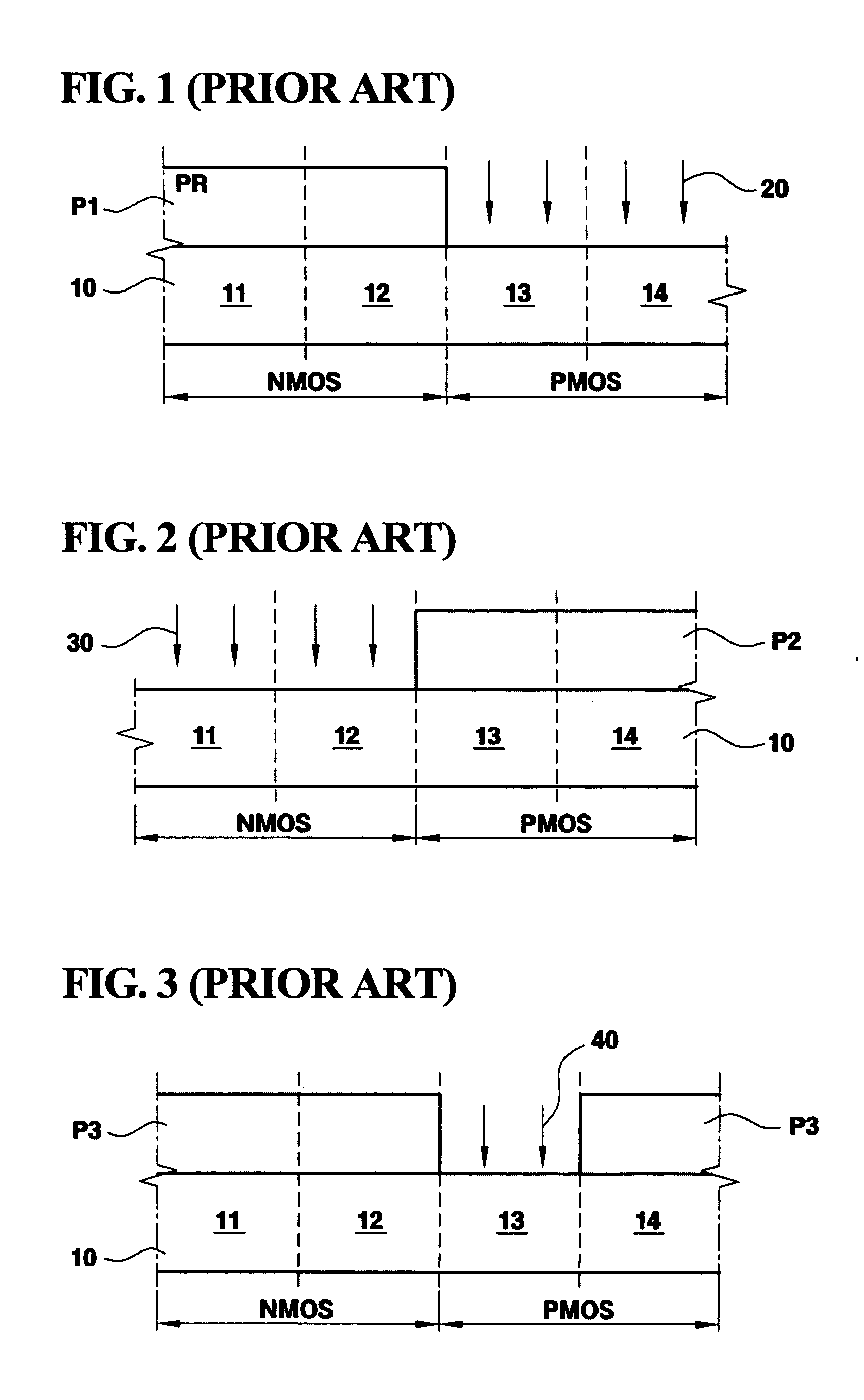
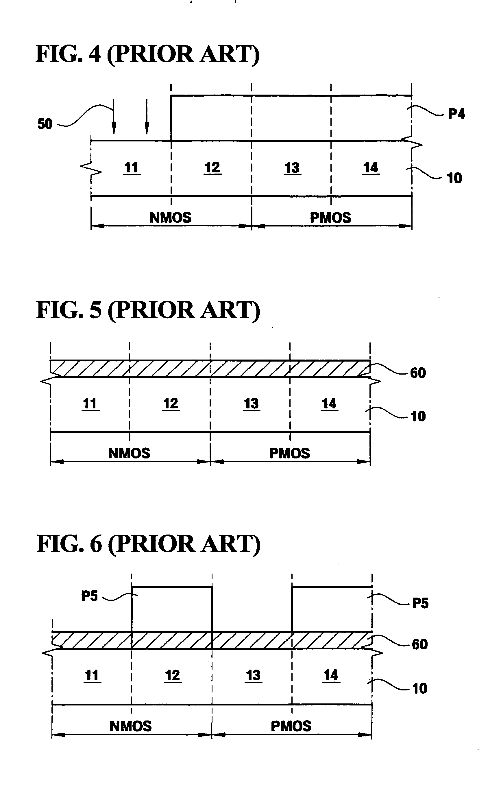
[0042] Referring to FIG. 8, a first photoresist (PR) is coated on a substrate 100 having NMOS forming regions 110 and 120 and PMOS forming regions 130 and 140. The first PR is then patterned by photolithography to form a first PR pattern P1 on the substrate 100 to cover the NMOS forming regions 110 and 120 and to expose the PMOS forming regions 130 and 140. A first conductivity type impurity 210 for forming an N well and a second conductivity type impurity 220 for controlling a threshold voltage (Vth) are sequentially implanted into the exposed PMOS forming regions 130 and 140 using the first PR pattern P1 as a...

second embodiment

[0064] A method of fabricating a dual gate oxide of a semiconductor device according to the present invention will now be explained with reference to FIGS. 14 through 19.

[0065]FIGS. 14 through 19 illustrate cross-sectional views of sequential stages in a method of fabricating a dual gate oxide of a semiconductor device according to the second embodiment of the present invention.

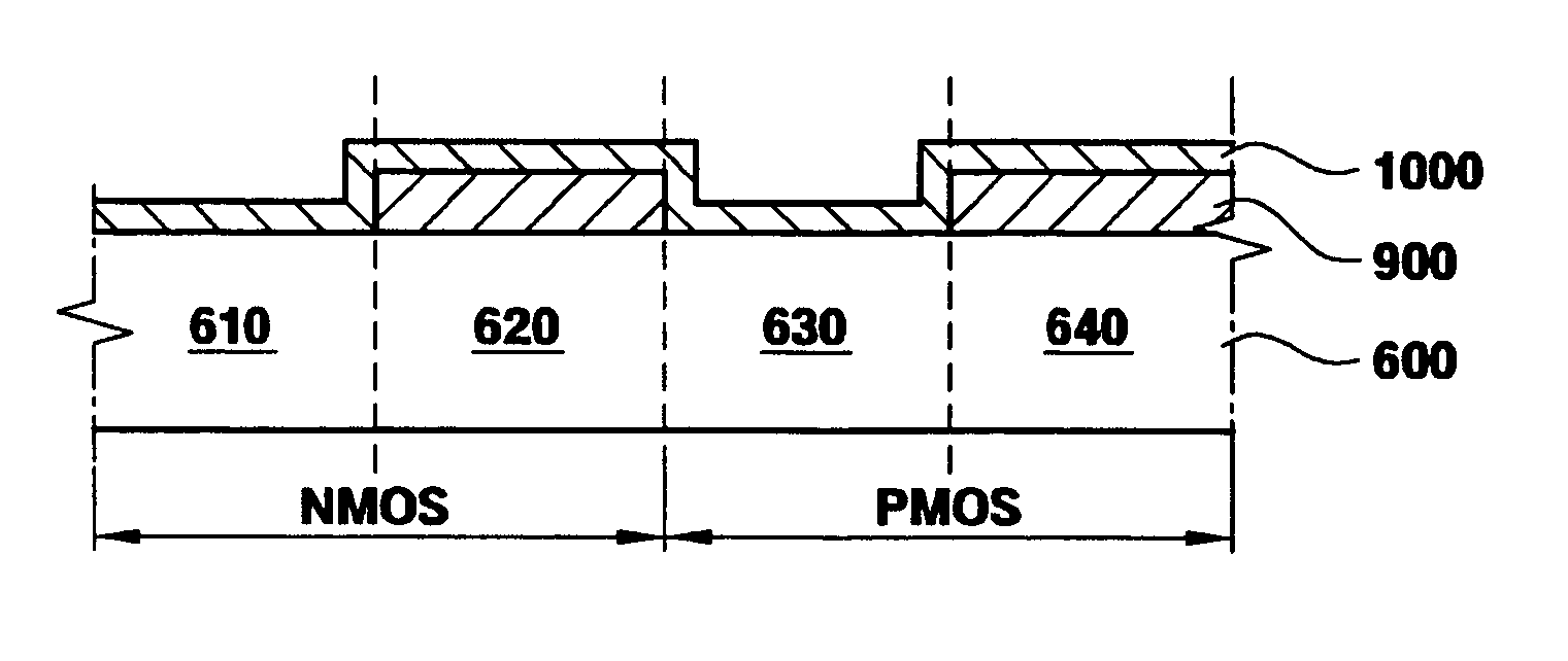
[0066] Referring to FIG. 14, a first photoresist (PR) is coated on a substrate 600 having first and second NMOS forming regions 610 and 620 and first and second PMOS forming regions 630 and 640. The first PR is patterned by photolithography to form a first PR pattern P1 on the substrate 600. The first PR pattern P1 covers the first and second NMOS forming regions 610 and 620 and the first PMOS forming region 630 and exposes the second PMOS forming region 640.

[0067] A first conductivity type impurity 710 for forming an N well and a second conductivity type impurity 720 for controlling a threshold voltage (Vt...


PUM


Abstract

A method of fabricating a dual gate oxide of a semiconductor device includes forming a first gate insulation layer over an entire surface of a substrate, removing a portion of the first gate insulation layer to selectively expose a first region of the substrate using a first mask and performing an ion implantation on the selectively exposed first region of the substrate using the first mask, and forming a second gate insulation layer on the first gate insulation layer and the exposed first region of the substrate to form a resultant gate insulation layer having a first thickness over the first region of the substrate and a second thickness over a remaining region of the substrate, the first thickness and the second thickness being different.

Description

BACKGROUND OF THE INVENTION [0001] 1. Field of the Invention [0002] The present invention relates to a method of fabricating a dual gate oxide of a semiconductor device. More particularly, the present invention relates to a method of forming a resultant gate oxide layer having a varying thickness on a single chip for fabricating a metal oxide semiconductor (MOS) device having different operating voltages. [0003] 2. Description of the Related Art [0004] In general, an area of a chip where a thinner gate oxide is formed is used for a peripheral logic circuit requiring a high driving power, and an area of the same chip where a thicker gate oxide is formed is used for a memory cell circuit requiring a high breakdown voltage characteristic. [0005] In order to implement MOS devices driven by different operating voltages in a single chip, rather complex photolithographic etching processes are required. For example, a step of forming gate oxide layers having different thicknesses and a step...

Claims


Application Information

Patent Timeline
IPC IPC(8): H01L21/8238H01L21/336
CPCH01L21/823857E05B3/00E05B9/02
Inventor LEE, HYAE-RYOUNGBAE, SU-GON
Owner SAMSUNG ELECTRONICS CO LTD
Features
  • Generate Ideas
  • Intellectual Property
  • Life Sciences
  • Materials
  • Tech Scout
  • Unparalleled Data Quality
  • Higher Quality Content
  • 60% Fewer Hallucinations
Learn More