Low resistance T-gate MOSFET device using a damascene gate process and an innovative oxide removal etch

a damascene gate and low resistance technology, applied in the field of low resistance damascene gate metal oxide semiconductor field effect transistor (mosfet) devices, can solve the problems of reducing device performance, increasing the number of mosfet devices with high yield and reliability, and increasing the integration of mosfet devices with high sheet resistan

Inactive Publication Date: 2005-08-04
IBM CORP
View PDF12 Cites 22 Cited by
  • Summary
  • Abstract
  • Description
  • Claims
  • Application Information

AI Technical Summary

Benefits of technology

[0015] forming nitride spacers on exposed vertical sidewalls of said recessed poly-gate that are beneath said gate conductor.
[0020] nitride spacers located on expose

Problems solved by technology

Over the past twenty-five years or so, the primary challenge of VLSI (very large scale integration) has been the integration of an ever-increasing number of MOSFET devices with high yield and reliability.
For high performance 0.1 μm CMOS devices, the conventional proc

Method used


Image

  • Low resistance T-gate MOSFET device using a damascene gate process and an innovative oxide removal etch
  • Low resistance T-gate MOSFET device using a damascene gate process and an innovative oxide removal etch
  • Low resistance T-gate MOSFET device using a damascene gate process and an innovative oxide removal etch

Examples


Embodiment Construction

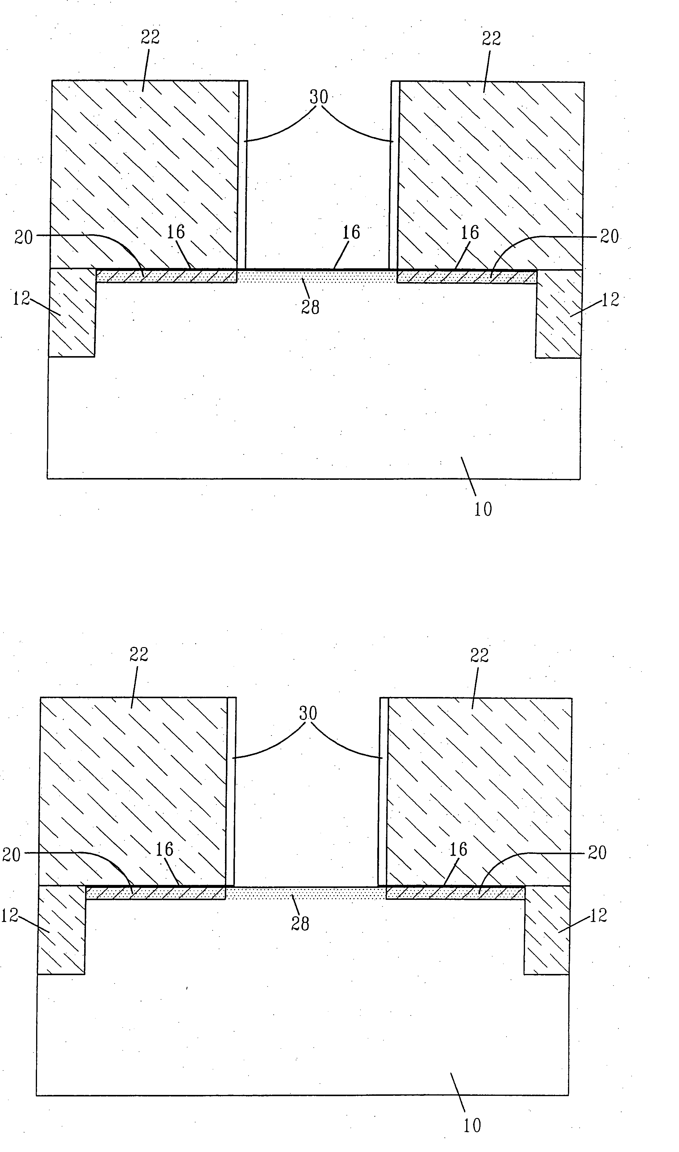
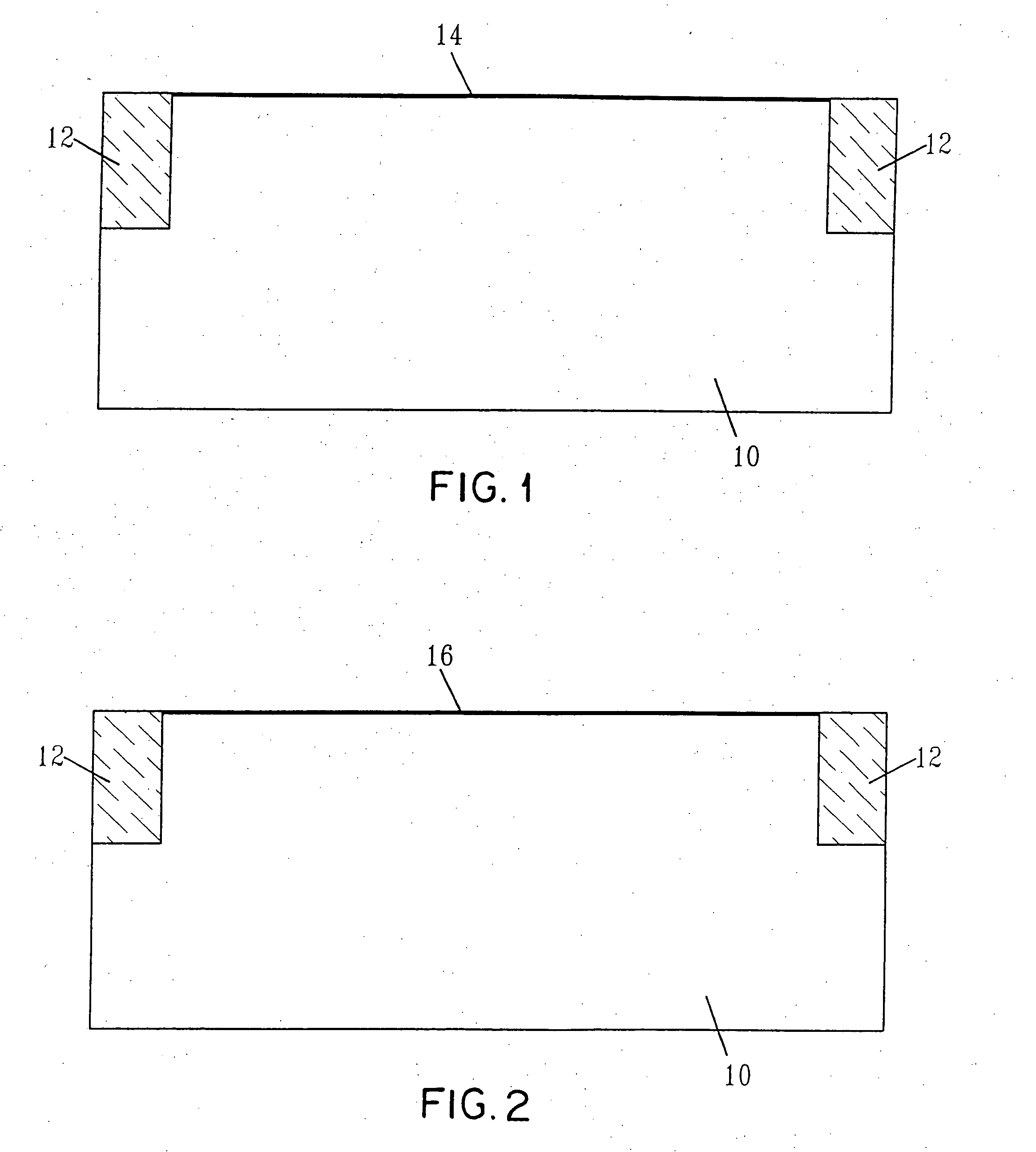
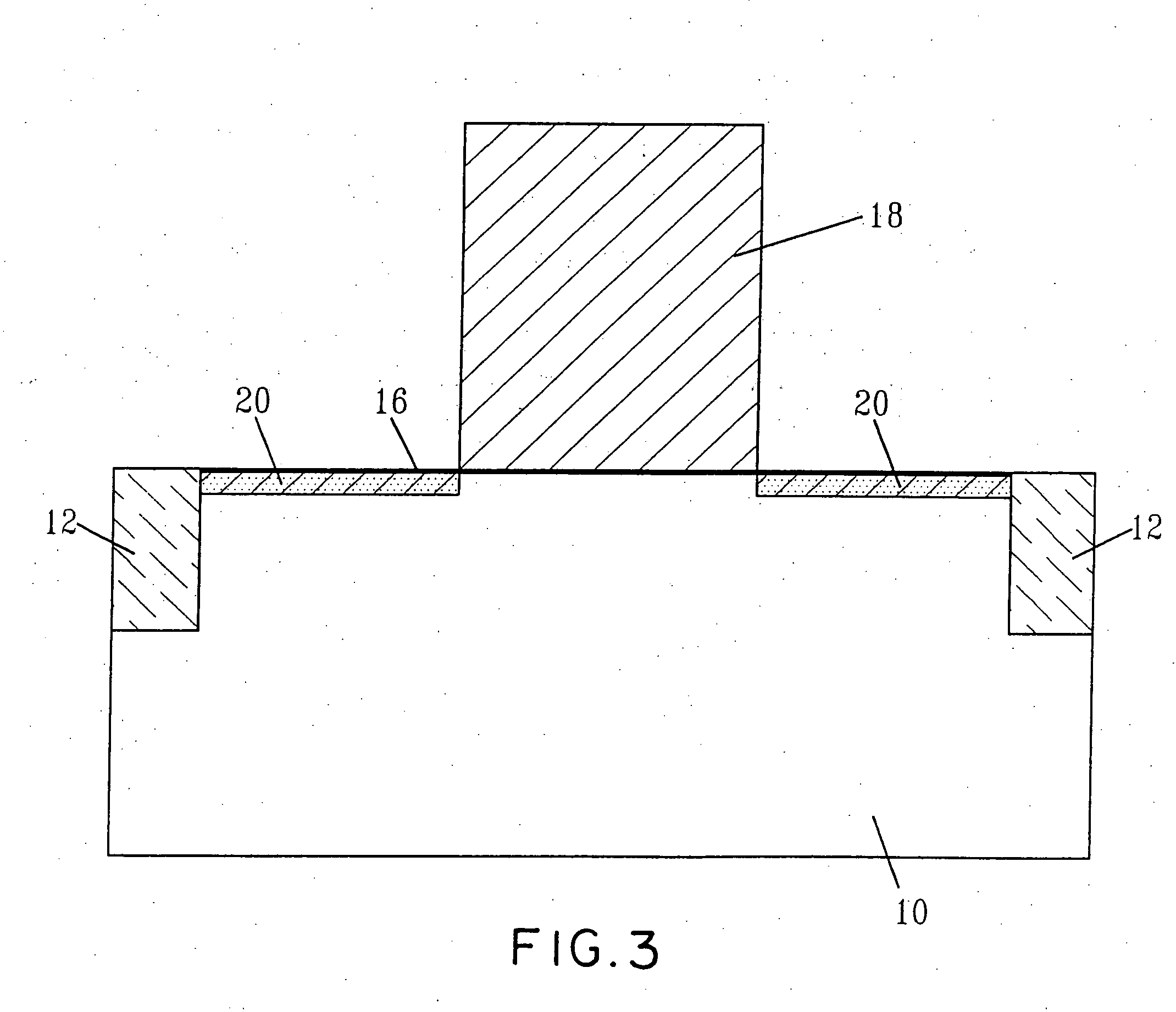
[0022] The present invention, which provides a method for fabricating a low-resistance T-gate MOSFET device, will now be described in more detail by referring to the drawings that accompany the present application.

[0023]FIG. 1 shows an initial structure that is employed in the present invention. Specifically, the initial structure shown in FIG. 1 comprises Si-containing substrate 10 having isolation regions 12 formed therein as well as pad oxide layer 14 located atop a surface of Si-containing substrate 10. The term “Si-containing is used in the present application to denote a material that includes silicon. Illustrate examples of such Si-containing substrates include, but are not limited to: Si, SiGe, SiGeC, SiC, Si / Si, Si / SiC, Si / SiGeC and Si-on-insulator (SOI) where substrate 10 is the top Si-containing layer of the SOI substrate. In the case of SOI substrates, the SOI substrate will include a buried oxide region beneath the top Si-containing layer which serves to electrically i...


PUM


Abstract

The present invention provides a method for fabricating low-resistance, sub-0.1 μm channel T-gate MOSFETs that do not exhibit any poly depletion problems. The inventive method employs a damascene-gate processing step and a chemical oxide removal etch to fabricate such MOSFETs. The chemical oxide removal may be performed in a vapor containing HF and NH3 or a plasma containing HF and NH3.

Description

FIELD OF THE INVENTION [0001] The present invention relates to semiconductor devices, and more particularly to a low-resistance, damascene T-gate metal oxide semiconductor field effect transistor (MOSFET) device. The present invention also relates to a method of fabricating a low-resistance, damascene T-gate MOSFET which uses damascene-gate processing as well as an innovative oxide removal etch. BACKGROUND OF THE INVENTION [0002] Over the past twenty-five years or so, the primary challenge of VLSI (very large scale integration) has been the integration of an ever-increasing number of MOSFET devices with high yield and reliability. This was achieved mainly by scaling down MOSFET gate / channel length, reducing gate dielectric thickness and increasing channel doping concentration. [0003] In conventional complementary metal oxide semiconductor (CMOS) processes, the source, drain and gate regions of the MOSFET are implanted, activated annealed and thereafter silicided so as to produce low...

Claims


Application Information

Patent Timeline
IPC IPC(8): H01L21/28H01L21/336H01L29/423H01L29/78
CPCH01L21/28114H01L29/42376H01L29/7833H01L29/66553H01L29/6659H01L29/66545H01L29/6653
Inventor HANAFI, HUSSEIN I.NATZLE, WESLEY
Owner IBM CORP
Why Eureka
Try Eureka